
Array substrate, display panel, and display device

Active Publication Date: 2021-09-16
SHENZHEN CHINA STAR OPTOELECTRONICS SEMICON DISPLAY TECH CO LTD
View PDF0 Cites 0 Cited by
  • Summary
  • Abstract
  • Description
  • Claims
  • Application Information

AI Technical Summary

Benefits of technology

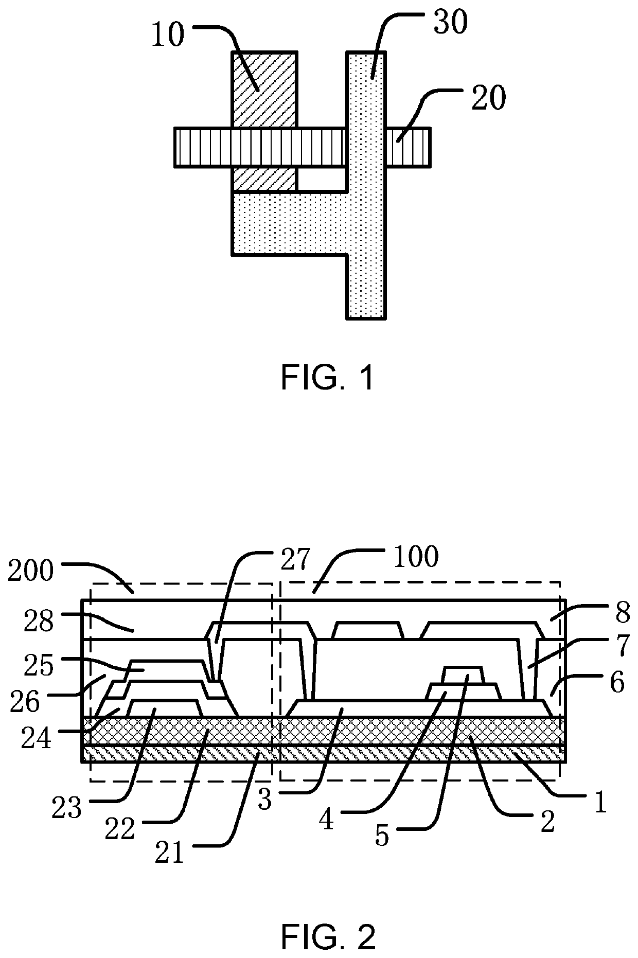
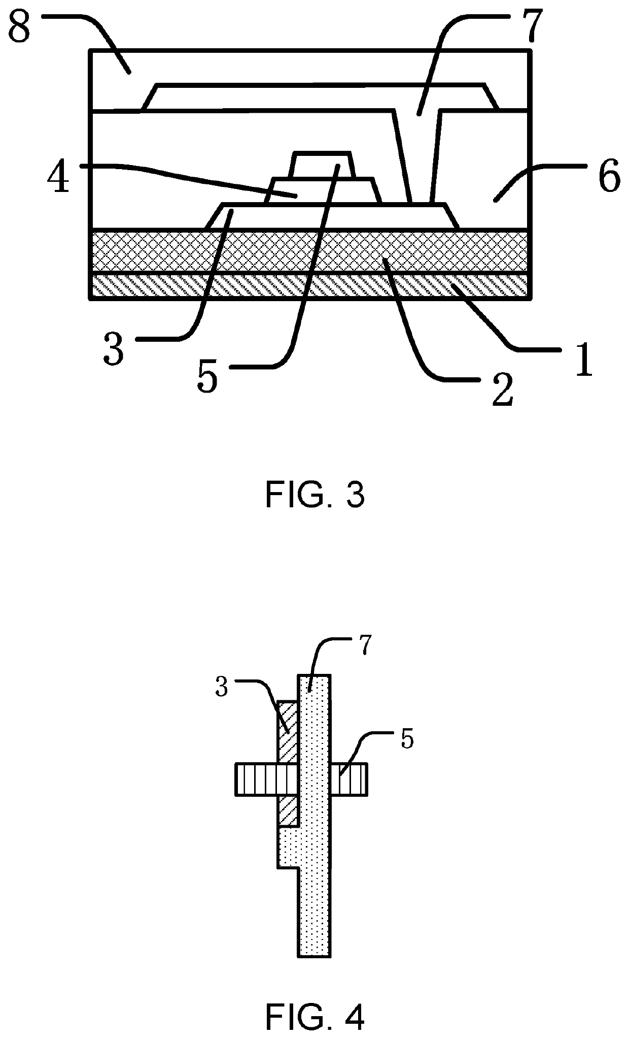
The present invention allows for the placement of semiconductor layers directly below data lines, without reserving design space in the display panel. This saves space and improves the space utilization of the pixel, which meets the requirements for high pixel density in display devices.

Problems solved by technology

However, the optimization of the manufacturing processes is affected by equipment capacities and panel yield, so a degree of the optimization is limited.

Method used


Image

  • Array substrate, display panel, and display device
  • Array substrate, display panel, and display device

Examples


Embodiment Construction

[0024]In combination with accompanying drawings in embodiments of the present disclosure below, technical solutions in the embodiments of the present disclosure are clearly and completely described. Obviously, the described embodiments are merely a part of the embodiments of the present disclosure, rather than all the embodiments. Based on the embodiments in the present disclosure, all of other embodiments obtained by those skilled in the art without making for creative efforts belong to the scope protected by the present disclosure.

[0025]In the description of the present disclosure, it should be understood that indicative directions or position relations, such as terms “center”, “longitudinal”, “transverse”, “length”, “width”, “thickness”, “upper”, “lower”, “front”, “back”, “left”, “right”, “vertical”, “horizontal”, “top”, “bottom”, “inner”, “outer”, “clockwise”, and “counterclockwise”, are based on directions or position relations indicated by the accompanying drawings. The indica...


PUM


Abstract

An array substrate, a display panel, and a display device are provided. The array substrate includes a substrate, a semiconductor layer, a gate insulation layer, a gate layer, an interlayer insulation layer, and data lines, wherein the semiconductor layer is directly below the data lines.

Description

FIELD OF INVENTION[0001]The present disclosure relates to the field of display, and in particular, to an array substrate, a display panel, and a display device.BACKGROUND OF INVENTION[0002]As a requirement for pixel density in organic light-emitting diode (OLED) display panels increases, a size of the pixel is gradually reduced, such that design space in the pixel is compressed. Hence, in the limited space, realizing rational designs of array substrates has become an important consideration.[0003]Currently, optimization of manufacturing processes is an important consideration. By shortening a width of metal lines and a distance between the metal lines, more space meets designing requirements for the array substrates. However, the optimization of the manufacturing processes is affected by equipment capacities and panel yield, so a degree of the optimization is limited.[0004]FIG. 1 is a schematic view of an array substrate of a display device in conventional technology. A semiconducto...

Claims


Application Information

Patent Timeline
IPC IPC(8): H01L27/32
CPCH01L27/3276H10K59/1213H10K59/131
Inventor ZHOU, SHUAIXUE, YAN
Owner SHENZHEN CHINA STAR OPTOELECTRONICS SEMICON DISPLAY TECH CO LTD
Learn More