High power LED chip back electrode integrated package module with stand

a technology of led chip back electrodes and integrated packaging, which is applied in the direction of semiconductor devices for light sources, light and heating apparatus, planar light sources, etc., can solve the problems of led chip damage and potential safety hazards, and achieve the effects of convenient replacement, convenient assembly and firm structur

Inactive Publication Date: 2021-03-18
SHENZHEN BLUE SPECTRUM RICK TECH CO LTD
View PDF0 Cites 0 Cited by
  • Summary
  • Abstract
  • Description
  • Claims
  • Application Information

AI Technical Summary

Benefits of technology

[0021](1) The module of the invention is simple and firm in structure, easy to assemble and convenient to replace, thus saving time;
[0022](2) The ceramic layer improves the heat dissipation effect and the operating stability and is resistant to high temperature and aging, thus having a longer service life;
[0023](3) The electrode terminal blocks are isolated from the outside and are prevented from being contaminated by external impurities, so that the electrode terminal blocks are better protected, the service life of products is prolonged, the products can be used more safely, the stability of the products is improved, and the high voltage isolation requirements of electronic products are satisfied;
[0024](4) The electrode terminal blocks are connected to external components by crimping, so that the process is made simpler and faster; and
[0025](5) The lens made of glass guarantees the light output efficiency, better protects the LED chips, is not prone to aging, simplifies the structure of products, is convenient to clean, and saves costs.

Problems solved by technology

The electrode terminal blocks of existing high-power LED chip packaging modules are disposed on a circuit layer, namely the emergent sides of LED chips, and are connected to external components by welding, which has the detects that the electrode terminal blocks exposed to the outside may be contaminated by external impurities and even short circuits between the electrode terminal blocks may be caused, thus resulting in damage to the LED chips and potential safety hazards.

Method used


Image

  • High power LED chip back electrode integrated package module with stand
  • High power LED chip back electrode integrated package module with stand
  • High power LED chip back electrode integrated package module with stand

Examples


Embodiment Construction

[0035]For the sake of a better understanding of the technical issues to be settled by the invention as well as the technical solutions and beneficial effects of the invention, the invention is further expounded below in conjunction with the accompanying drawings and embodiments. Understandably, the specific embodiments described hereinafter are only used to explain the invention, and are not intended to limit the invention.

[0036]It should be noted that when one element is erred to as being “connected to” another element, this element is directly or indirectly connected to the other element. Moreover, the terms “first” and “second” are used only for the purpose of description, and do not indicate or imply relative importance or implicitly specify the quantity of the technical features referred to. Therefore, a feature defined by “first” and “second” may clearly or implicitly indicate that one or more of the feature: are included.

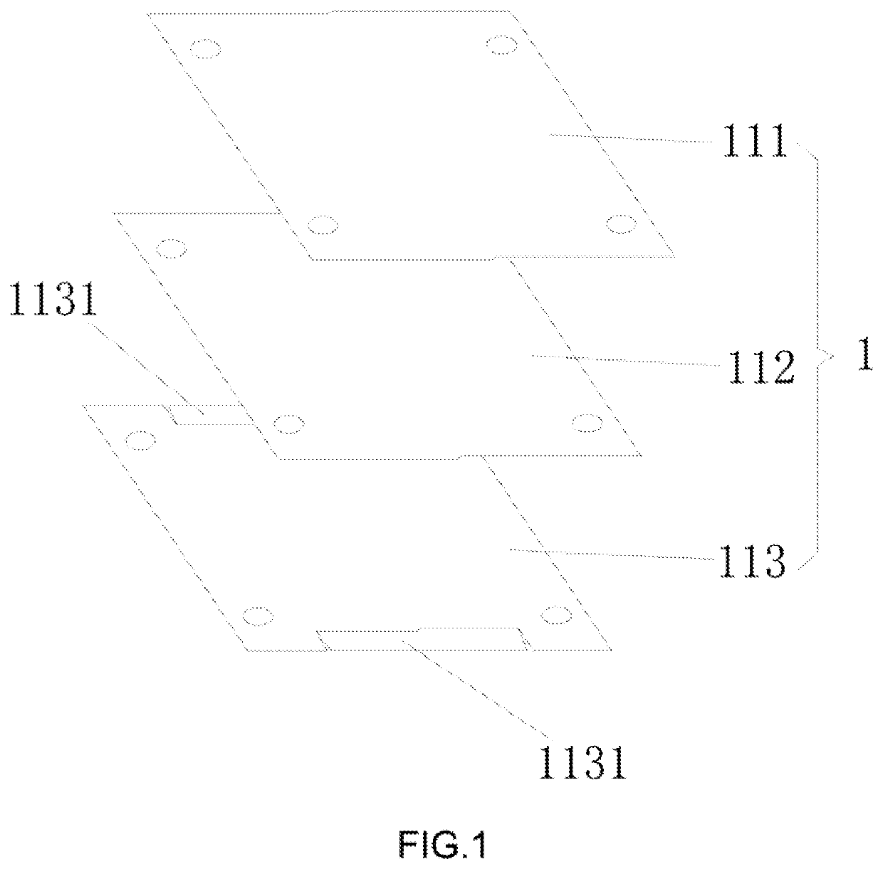
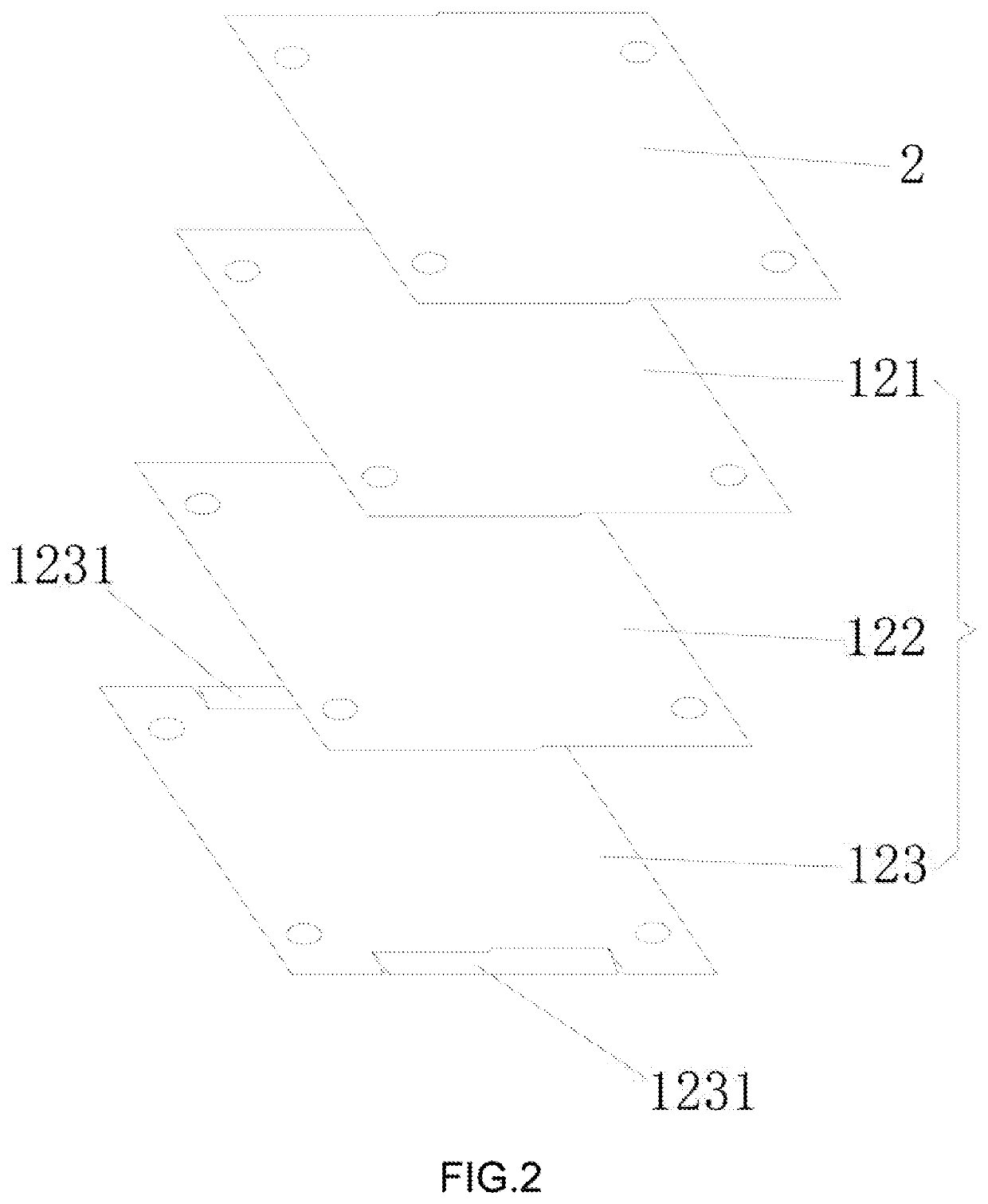
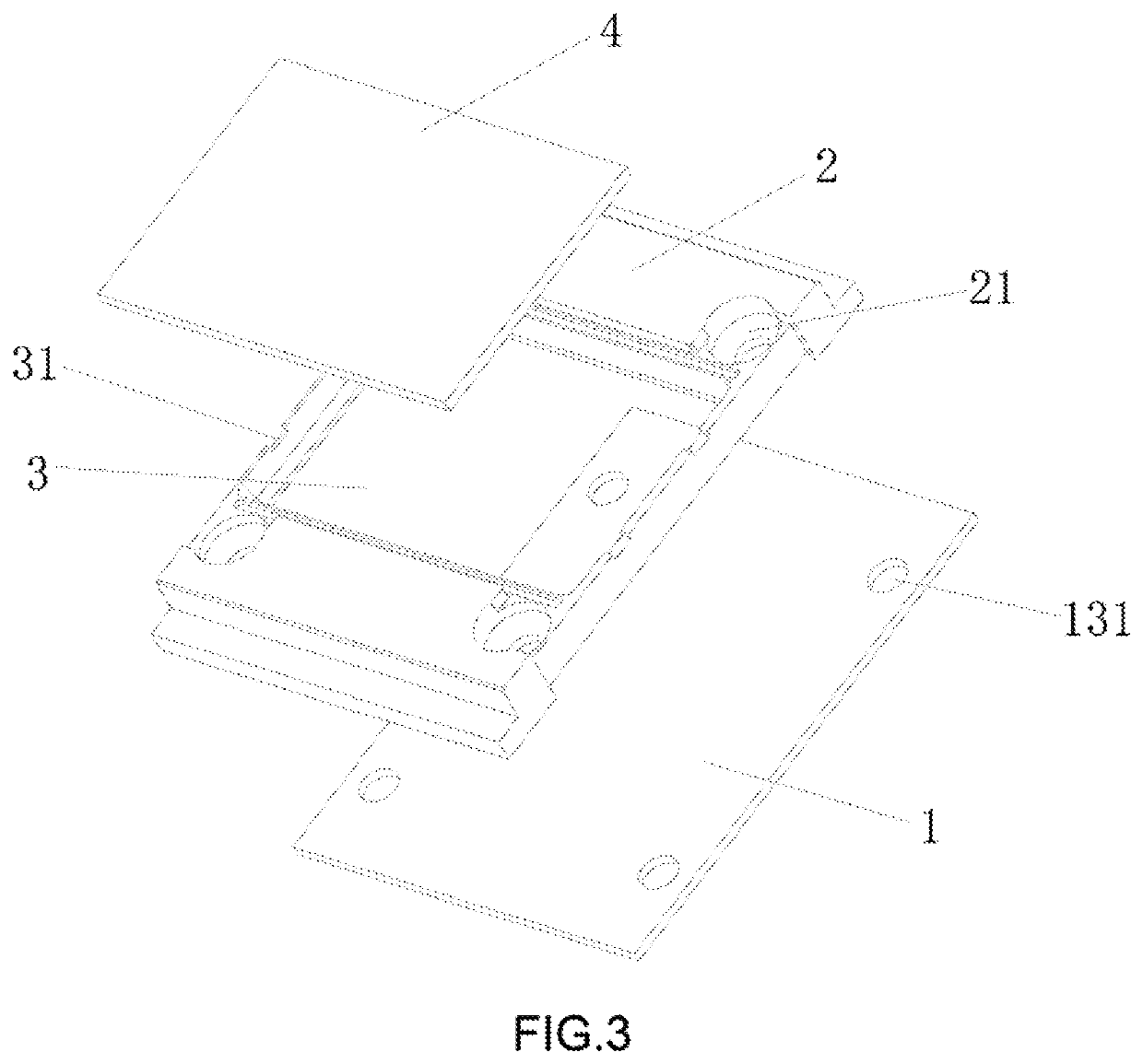
[0037]Referring to FIG. 1, FIG, and FIG. 7, a high-powe...


PUM

PropertyMeasurementUnit
poweraaaaaaaaaa
structureaaaaaaaaaa
operating stabilityaaaaaaaaaa

Abstract

The present invention provides a high power LED chip back electrode integrated package module with a stand, comprising a substrate, a lens stand, and a tens made of glasses. The lens stand is provided above the substrate and wraps same, and is provided with a fixed cavity where the lens is placed; the lens is provided in the fixed cavity and is connected to the lens stand; the substrate comprises a first line layer, a first ceramic layer, and a first metal layer which are connected sequentially; a first electrode connection disk is provided at both ends of the first metal layer; the first electrode connection disk is connected to the first line layer, and is in pressure connection to an external component; the first line layer is provided with multiple first LED chip units; the lens is provided above the first LED chip units and corresponds to the position thereof. The present invention further provide another high power LED chip back electrode integrated package module with a stand. According to the present invention, the electrode connection disk is isolated from the outside to prevent external impurities from contaminating the electrode connection disk.

Description

BACKGROUND OF THE INVENTION[0001]The invention relates to a high-power LED chip back electrode integrating and packaging module provided with a holder.[0002]The electrode terminal blocks of existing high-power LED chip packaging modules are disposed on a circuit layer, namely the emergent sides of LED chips, and are connected to external components by welding, which has the detects that the electrode terminal blocks exposed to the outside may be contaminated by external impurities and even short circuits between the electrode terminal blocks may be caused, thus resulting in damage to the LED chips and potential safety hazards.[0003]Hence, improvements should be made to overcome the above-mentioned defects.BRIEF SUMMARY OF THE INVENTION[0004]One objective of the invention is to overcome the defects of the prior art by providing a high-power LED chip back electrode integrating aid packaging module provided with a holder.[0005]The technical solution of the invention is as follows:[0006...

Claims


Application Information

Patent Timeline
Patent Type & Authority Applications(United States)
IPC IPC(8): H01L33/38H01L33/58
CPCH01L33/382H01L33/483H01L33/387H01L33/58F21K9/00F21V5/007F21V5/008F21V5/041F21V5/043F21V17/12F21Y2105/16F21Y2115/10H01L25/0753
Inventor ZHANG, HESHENG
Owner SHENZHEN BLUE SPECTRUM RICK TECH CO LTD
Why Eureka
Try Eureka