Stacked lens structure and method of manufacturing the same, and electronic apparatus
a technology of stacked lens and manufacturing method, applied in the field of stacking lens structure and manufacturing method, can solve the problems of large lens thickness, low degree of freedom in shape, and variability in wafer plane accuracy, and achieve the effect of reducing size and not increasing the number of steps
- Summary
- Abstract
- Description
- Claims
- Application Information
AI Technical Summary
Benefits of technology
Problems solved by technology
Method used
Image

Examples
first embodiment
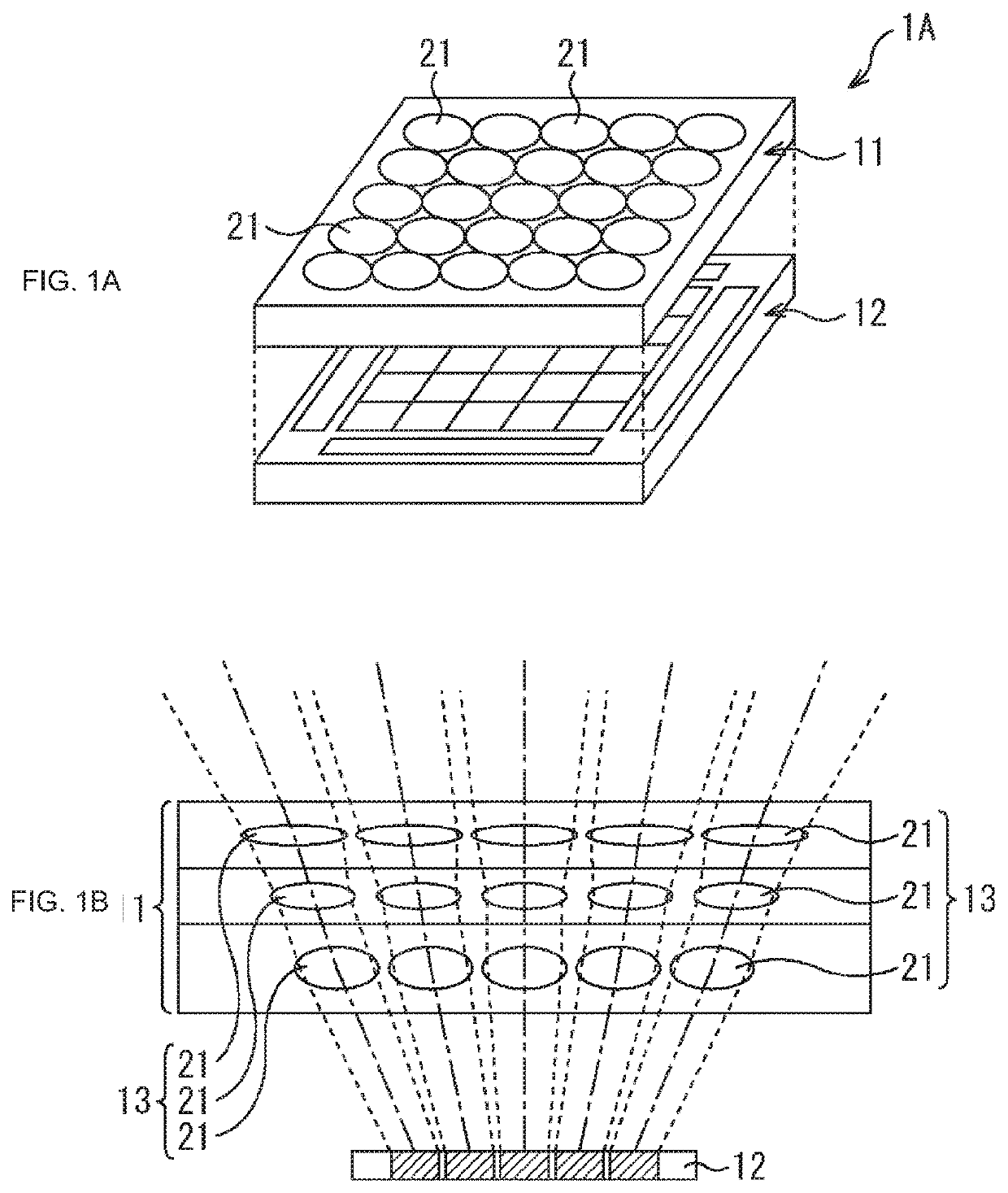
[0153]FIG. 1 illustrates figures depicting a first embodiment of a camera module using a stacked lens structure to which the present technology is applied.
[0154]In FIG. 1, A is a schematic view depicting a configuration of a camera module 1A as a first embodiment of a camera module 1. In FIG. 1, B is a schematic sectional view of the camera module 1A.
[0155]The camera module 1A includes a stacked lens structure 11 and a light receiving element 12. The stacked lens structure 11 includes a total of 25 optical units 13, five in a column direction and five in a row direction. The optical unit 13 includes plural lenses 21 in a single optical axis direction. The camera module 1A is a multiple-lensed camera module having a multiplicity of optical units 13.
[0156]The optical axes of the multiplicity of optical units 13 possessed by the camera module 1A are disposed to be widened toward the outside of the module, as depicted in B in FIG. 1, whereby wide-angle imaging can be performed.
[0157]Not...
second embodiment
[0194]FIG. 9 illustrates figures depicting a second embodiment of the camera module using the stacked lens structure to which the present technology is applied.
[0195]In FIG. 9, A is a schematic view depicting an external appearance of a camera module 1B as the second embodiment of the camera module 1. In FIG. 9, B is a schematic sectional view of the camera module 1B.
[0196]The camera module 1B includes two optical units 13. The two optical units 13 each include a diaphragm plate 51 at an uppermost layer of a stacked lens structure 11. The diaphragm plate 51 is provided with an opening 52.
[0197]While the camera module 1B includes the two optical units 13, the two optical units 13 differ in optical parameters. In other words, the camera module 1B includes two kinds of optical units 13 differing in optical performance. The two kinds of optical units 13 may be, for example, an optical unit 13 having a shorter focal distance for imaging a close-range view, and an optical unit 13 having a...
third embodiment
[0203]FIG. 10 illustrates figures depicting a third embodiment of the camera module using the stacked lens structure to which the present technology is applied.
[0204]In FIG. 10, A is a schematic view depicting an external appearance of a camera module 1C as the third embodiment of the camera module 1. In FIG. 10, B is a schematic sectional view of the camera module 1C.
[0205]The camera module 1C includes a total of four optical units 13, two in a column direction and two in a row direction, on a light incidence surface. The four optical units 13 are the same with one another in the shape of the lenses 21.
[0206]While the four optical units 13 each include a diaphragm plate 51 at an uppermost layer of a stacked lens structure 11, the four optical units 13 are different from one another in the size of an opening 52 formed in the diaphragm plate 51. As a result, the camera module 1C may realize, for example, the following camera module 1C. Specifically, for example, in a monitoring camer...
PUM
 Abstract
Description
Claims
Application Information
 - R&D
- Intellectual Property
- Life Sciences
- Materials
- Tech Scout
- Unparalleled Data Quality
- Higher Quality Content
- 60% Fewer Hallucinations
Browse by: Latest US Patents, China's latest patents, Technical Efficacy Thesaurus, Application Domain, Technology Topic, Popular Technical Reports.
© 2025 PatSnap. All rights reserved.Legal|Privacy policy|Modern Slavery Act Transparency Statement|Sitemap|About US| Contact US: help@patsnap.com