
Planar Optical Waveguide Based on Two-Dimensional Optical Gratings

Active Publication Date: 2020-08-20
SHANGHAI NORTH OCEAN TECH CO LTD
View PDF0 Cites 1 Cited by
  • Summary
  • Abstract
  • Description
  • Claims
  • Application Information

AI Technical Summary

Benefits of technology

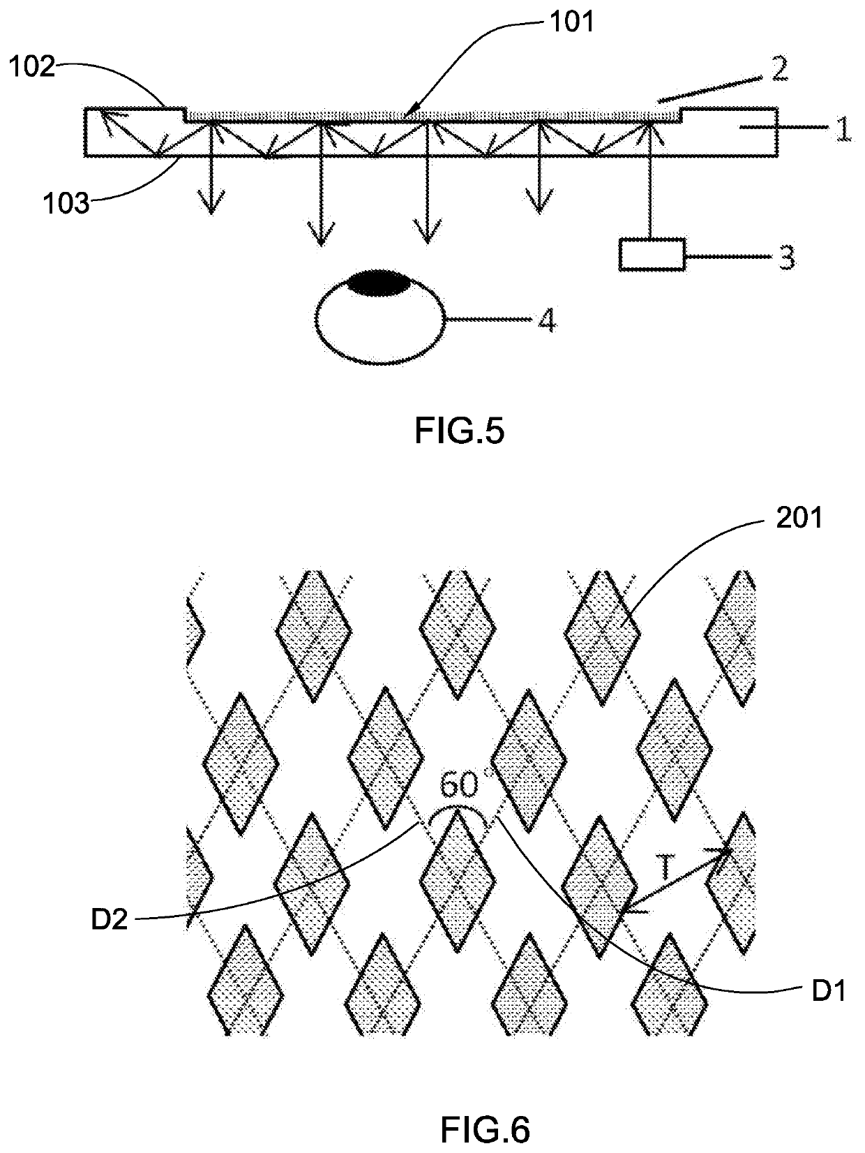
The present invention is for a planar optical waveguide that uses a two-dimensional grating to efficiently couple micro-projectors with optical waveguides. The optical waveguide substrate is a transparent plate with a functional grating element consisting of a two-dimensional grating with an angle of 60 degrees. The grating can be protruding from the substrate or etched into it. This design provides flexibility in the input and output of light, reducing the alignment tolerance between the optical waveguide and the micro-projector, expanding the visible area, and reducing manufacturing cost. Additionally, the grating can have modulated depths and shapes to improve the intensity uniformity of the output image. The grating is a monolithic structure suitable for mass-production and adaption.

Problems solved by technology

Since the free-form prism cannot be too thin due to its optical power requirement, the form factor of this solution is not compact enough for an ideal near-eye glass-like augmented reality display.
In these types of conventional planar optical waveguides, the optical components for image in-coupling, exit pupil expansion, and image out-coupling needs to be designed and manufactured separately, and therefore the manufacturability being low and manufacturing cost being high are two major drawbacks for this type of conventional planar optical waveguides.

Method used


Image

  • Planar Optical Waveguide Based on Two-Dimensional Optical Gratings
  • Planar Optical Waveguide Based on Two-Dimensional Optical Gratings
  • Planar Optical Waveguide Based on Two-Dimensional Optical Gratings

Examples


example 1

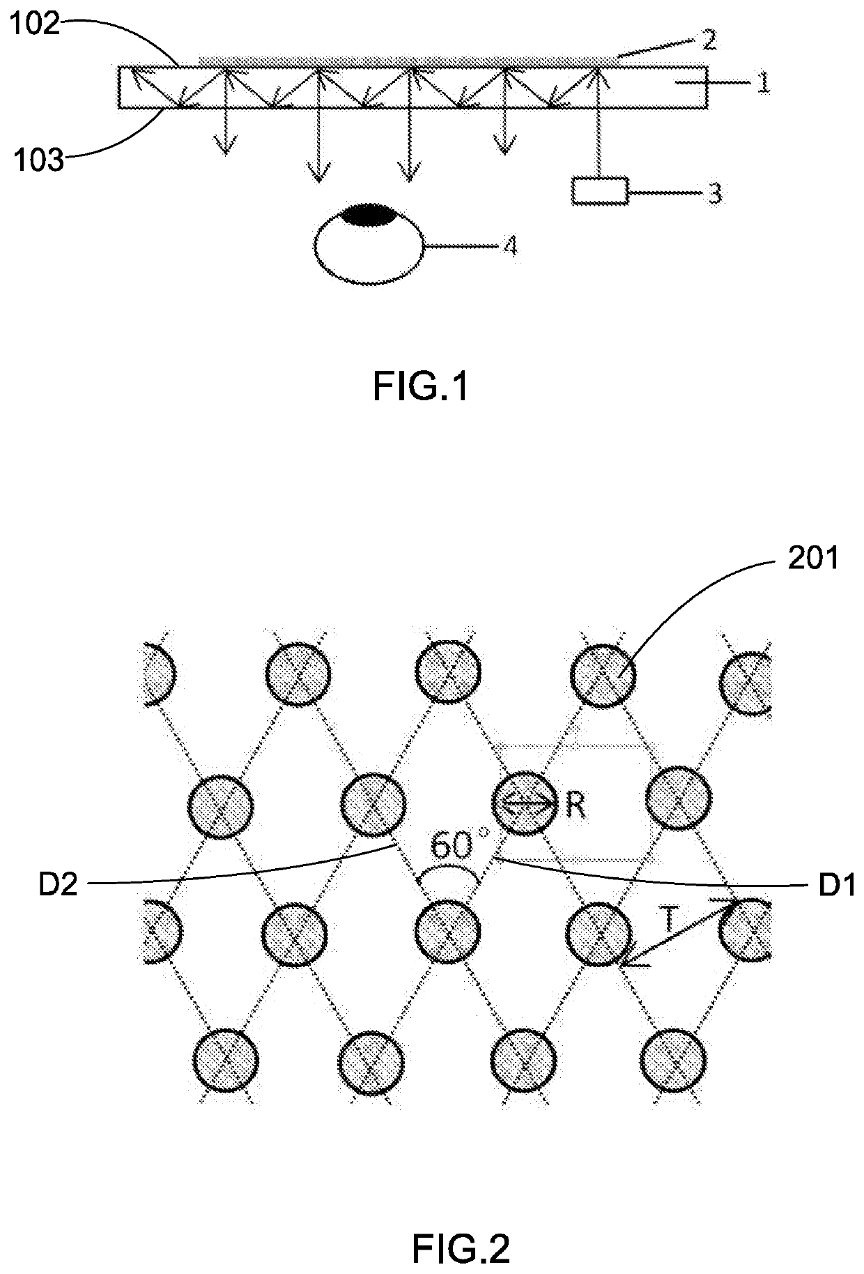
[0043]As shown in FIGS. 1 and 2, the planar optical waveguide based on the two-dimensional grating of this example of the present invention includes an optical waveguide substrate 1 and a functional grating element 2.

[0044]In this example, the optical waveguide substrate 1 is a plane-parallel glass plate with top surface 102 and bottom surface 103 being in parallel with each other. The thickness of the substrate is 0.5 mm. The refractive index of the substrate is 1.5.

[0045]A two-dimensional grating, which comprises a plurality of grating members 201 embodied as cylindrical columns, with an angle of 60° between the two grating directions, a period T of 360 nm, a column diameter R of 100 nm, and a depth of 150 nm, is formed on the surface of the plane-parallel glass plate (optical waveguide substrate 1) to work as the functional structure.

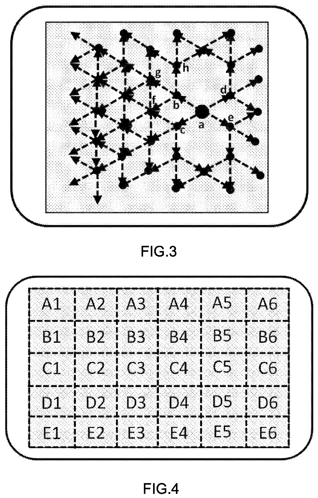
[0046]The optical waveguide is divided into 30 areas as shown in FIG. 4 with A to E along the vertical direction and 1 to 6 along the horizontal dir...

example 2

[0047]As shown in FIGS. 1 and 2, the planar optical waveguide based on the two-dimensional grating of this example of the present invention includes an optical waveguide substrate 1 and a functional grating element 2.[0048]In this example, the optical waveguide substrate 1 is a plane-parallel glass plate with top surface 102 and bottom surface 103 being in parallel with each other. The thickness of the substrate is 1.9 mm. The refractive index of the substrate is 1.8.

[0049]A two-dimensional grating, which comprises a plurality of grating members 201 embodied as diamond columns whose bottom cross section has a diamond shape, with an angle of 60° between the two grating directions, a period T of 450 nm, a side length of 200 nm, and a depth of 250 nm, is formed on the surface of the plane-parallel glass plate (optical waveguide substrate 1) to work as the functional structure.

[0050]The optical waveguide is divided into 30 areas with A to E along the vertical direction and 1 to 6 along ...

example 3

[0051]As shown in FIGS. 1 and 2, the planar optical waveguide based on the two-dimensional grating of this example of the present invention includes an optical waveguide substrate 1 and a functional grating element 2.

[0052]In this example, the optical waveguide substrate 1 is a plane-parallel glass plate with top surface 102 and bottom surface 103 being in parallel with each other. The thickness of the substrate is 0.5 mm. The refractive index of the substrate is 1.5.

[0053]A two-dimensional grating, which comprises a plurality of grating members 201 embodied as cylindrical columns, with an angle of 60° between the two grating directions, a period T of 360 nm, and a column diameter R of 100 nm, is formed on the surface of the plane-parallel glass plate (optical waveguide substrate 1) to work as the functional structure.

[0054]The intensity of light propagating inside the optical waveguide gradually decreases along with continuous out-coupling by the two-dimensional grating, and thus t...


PUM


Abstract

A planar optical waveguide based on two-dimensional grating includes an optical waveguide substrate which is a transparent plane-parallel plate, and a functional grating element which includes a two-dimensional grating having two grating directions with an angle of 60° in between. The two-dimensional grating is either protruded or recessed into the top surface of the optical waveguide substrate. The output image from a micro-projector can enter the optical waveguide and then gets projected to cover the entire area of the functional grating element, enabling a human eye to view the output image across a large eye-box.

Description

CROSS REFERENCE OF RELATED APPLICATION[0001]This application is a non-provisional application that claims priority under 35 U.S.C. § 119 to China application number CN201811597280.3, filed on Dec. 26, 2018, which is incorporated herewith by references in its entities.NOTICE OF COPYRIGHT[0002]A portion of the disclosure of this patent document contains material which is subject to copyright protection. The copyright owner has no objection to any reproduction by anyone of the patent disclosure, as it appears in the United States Patent and Trademark Office patent files or records, but otherwise reserves all copyright rights whatsoever.BACKGROUND OF THE PRESENT INVENTIONField of Invention[0003]The present invention relates to the technical field of augmented reality, and more particularly to a planar optical waveguide based on two-dimensional optical grating.Description of Related Arts[0004]The augmented reality technology, which is a new technology that integrates real world informati...

Claims


Application Information

Patent Timeline
IPC IPC(8): G02B6/124G02B27/01G02B27/00
CPCG02B2027/0125G02B27/0101G02B27/0081G02B6/124G02B27/0172G02B6/005G02B6/0026G02B6/0058G02B6/0065G02B2027/0178G02B6/00
Inventor HUANG, HELIN, TAOLOU, XINYE
Owner SHANGHAI NORTH OCEAN TECH CO LTD
Learn More