
Optimizing Junctions of Gate All Around Structures with Channel Pull Back

Active Publication Date: 2020-01-23
IBM CORP +1
View PDF5 Cites 8 Cited by
  • Summary
  • Abstract
  • Description
  • Claims
  • Application Information

AI Technical Summary

Benefits of technology

This patent describes a method for optimizing the junctions of a gate-all-around nanosheet device using channel pull back. The method involves forming an alternating stack of nanosheets and dummy gates, patterning the stack into fins, etching the fins to form pockets, filling the pockets with a strain-inducing material, selectively removing the dummy gate, and forming a replacement gate. The nanosheet device includes at least one fin stack with nanosheets and source and drains on its sides, with a strain-inducing material present in the fins. The technical effect of this patent is an improved performance of the nanosheet device by optimized junctions and better strain engineering.

Problems solved by technology

With current nanosheet device designs however, the source and the drains formed at the ends of the channels often have a high defect density, and thus have a limited effect on inducing compressive strain in the channels.

Method used


Image

  • Optimizing Junctions of Gate All Around Structures with Channel Pull Back
  • Optimizing Junctions of Gate All Around Structures with Channel Pull Back
  • Optimizing Junctions of Gate All Around Structures with Channel Pull Back

Examples


Embodiment Construction

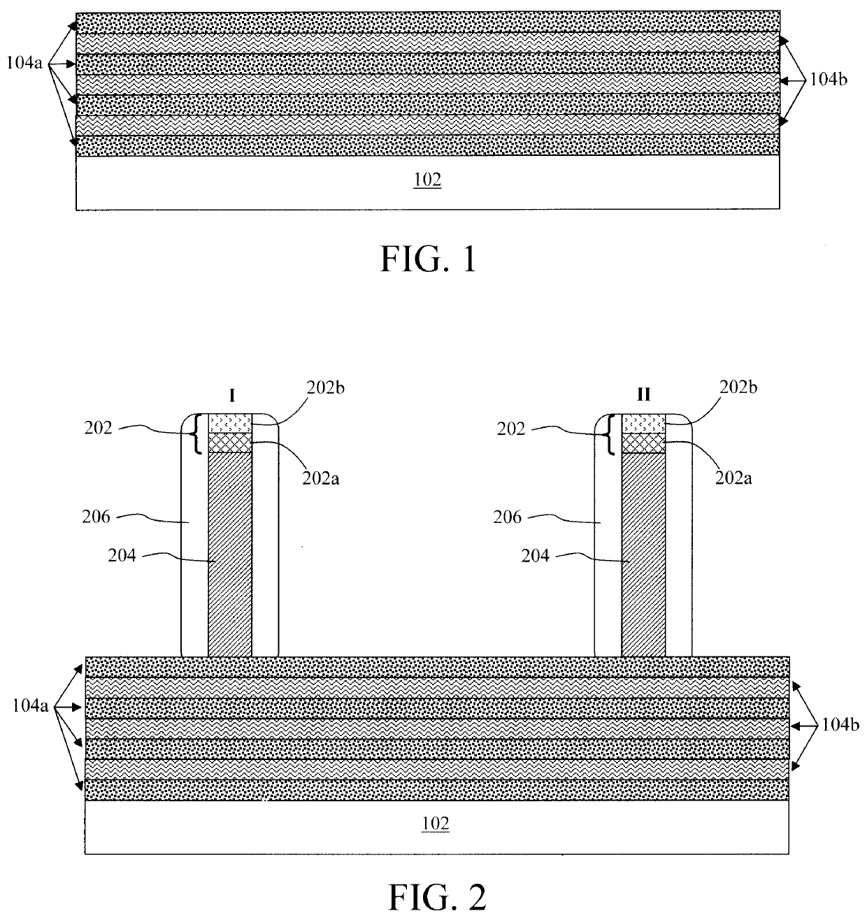
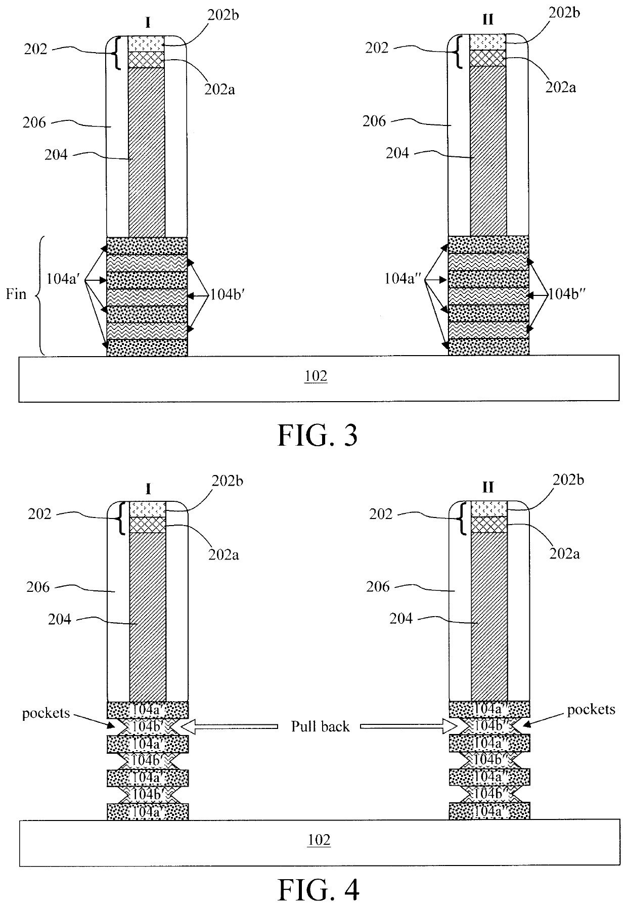
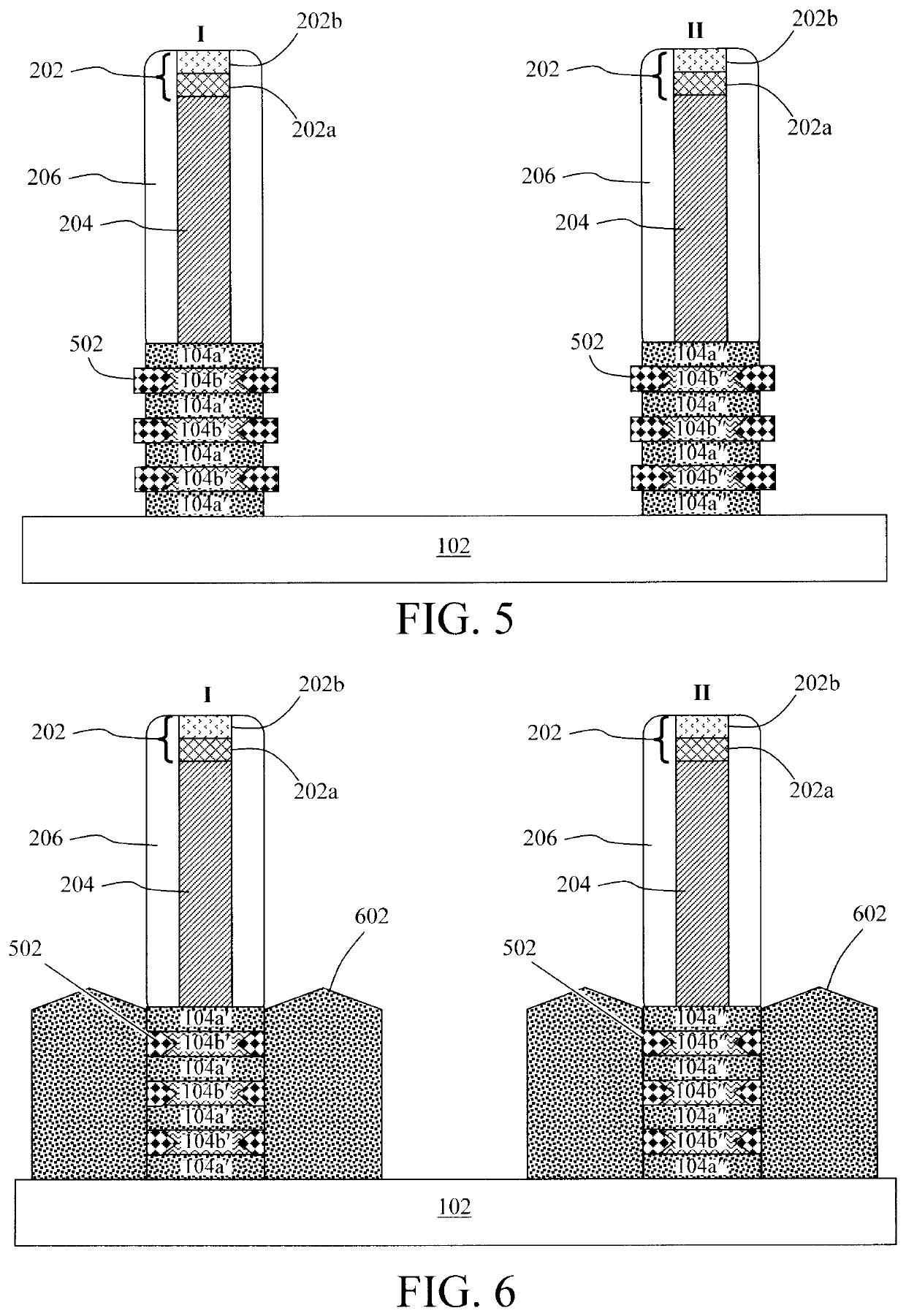
[0031]Provided herein are techniques for effectively inducing compressive strain on the nanosheet channels of a fin stack using channel pull back, wherein the nanosheet channels are etched back, forming pockets in the fin stack. A defect-free epitaxial material or tensile or compressive dielectric is then grown or deposited in the pockets straining the nanosheet channels. The nanosheet channels are then released from the stack, and a gate is formed surrounding a portion of each of the nanosheet channels in a gate-all-around (GAA) configuration.

[0032]As will be described in detail below, the starting structure for the present nanosheet devices is a stack of active channel layers alternating with sacrificial layers. By ‘sacrificial’ it is meant that the layer, or portion thereof, is removed during fabrication of the device. For instance, removal of the sacrificial layers from between channel layers serves to release the channel layers from the stack, thereby enabling the GAA configura...


PUM


Abstract

Techniques for optimizing junctions of a gate-all-around nanosheet device are provided. In one aspect, a method of forming a nanosheet device includes: forming an alternating series of first / second nanosheets including a first / second material as a stack on a wafer; forming a dummy gate(s) on the stack; patterning the stack into a fin stack(s) beneath the dummy gate(s); etching the fin stack(s) to selectively pull back the second nanosheets in the fin stack(s) forming pockets in the fin stack(s); filling the pockets with a strain-inducing material; burying the dummy gate(s) in a dielectric material; selectively removing the dummy gate(s) forming a gate trench(es) in the dielectric material; selectively removing either the first nanosheets or the second nanosheets from the fin stack(s); and forming a replacement gate(s) in the gate trench(es). A nanosheet device is also provided.

Description

FIELD OF THE INVENTION[0001]The present invention relates to gate-all-around (GAA) nanosheet devices, and more particularly, to techniques for optimizing junctions of a GAA nanosheet device using channel pull back.BACKGROUND OF THE INVENTION[0002]Nanosheet devices include a vertical stack of channel layers interconnecting a source and a drain. Advantageously, the channel layers are suspended between the source and the drain, thus enabling a gate-all-around (or GAA) design.[0003]A compressively-strained channel for p-channel field-effect transistors (p-FETs) serves to increase the hole mobility and thus enhance device performance. With current nanosheet device designs however, the source and the drains formed at the ends of the channels often have a high defect density, and thus have a limited effect on inducing compressive strain in the channels.[0004]Therefore, nanosheet device fabrication techniques that effectively induce compressive strain in the channel layers, and hence improv...

Claims


Application Information

Patent Timeline
IPC IPC(8): H01L21/8234H01L21/8238H01L29/66H01L29/06H01L29/78H01L29/423H01L27/088
CPCH01L21/823842H01L29/7848H01L29/7853H01L29/6653H01L21/823431H01L21/823412H01L27/0886H01L29/6681H01L21/3065H01L21/30604H01L29/0673H01L29/42392H01L29/66553H01L21/823807H01L21/823437H01L27/088H01L27/092H01L29/78696H01L29/66439H01L29/66772H01L29/66742H01L29/78654H01L29/78684H01L29/66545H01L29/0653H01L29/165H01L29/161H01L29/7843H01L29/775B82Y10/00H01L29/401H01L29/41725
Inventor LOUBET, NICOLASAUGENDRE, EMMANUELCOQUAND, REMIREBOH, SHAY
Owner IBM CORP
Learn More