A qubit apparatus and a qubit system

a qubit apparatus and apparatus technology, applied in the field of qubit apparatus and qubit system, can solve the problems of large interdigitated finger structure, difficult to retain enough control, fragile quantum information stored in the quantum state, etc., and achieve the effect of enhancing the capacitive embedding of the qubit, reducing the size, and facilitating coupling multiple other circuit elements

Active Publication Date: 2019-12-19
TECH UNIV DELFT
View PDF0 Cites 16 Cited by
  • Summary
  • Abstract
  • Description
  • Claims
  • Application Information

AI Technical Summary

Benefits of technology

The invention reduces the size of a transmon qubit and increases its coherence time by reducing electric fields in dielectrics. Connecting the qubit to other circuit elements is easier because the electric fields are confined between the two plates. The qubit can be controlled by a transmission line or transmission line resonator and can be shielded from unwanted cross-couplings. The qubit is capacitively embedded in the circuit, making it easier to control its coupling to various circuit elements and to protect the quantum information from decoherence. The quantum memory enhances the time that quantum information can be stored without being lost and also allows different protocols to protect the quantum state. Overall, the invention improves the performance and reliability of quantum information processing.

Problems solved by technology

A mayor engineering hurdle is the fact that the quantum information stored in the quantum state is very fragile to unwanted and uncontrolled environmental influences, known as decoherence.
Combining both, preventing decoherence, whilst retain enough control is challenging.
A drawback of this transmon qubit system according to prior art is the large size of the interdigitated finger structure (Super conducting islands 1 and 2), as a quantum computer needs multiple qubits and the interdigitated finger structure (Super conducting islands 1 and 2) is large, about 290 μm.

Method used


Image

  • A qubit apparatus and a qubit system
  • A qubit apparatus and a qubit system
  • A qubit apparatus and a qubit system

Examples


Embodiment Construction

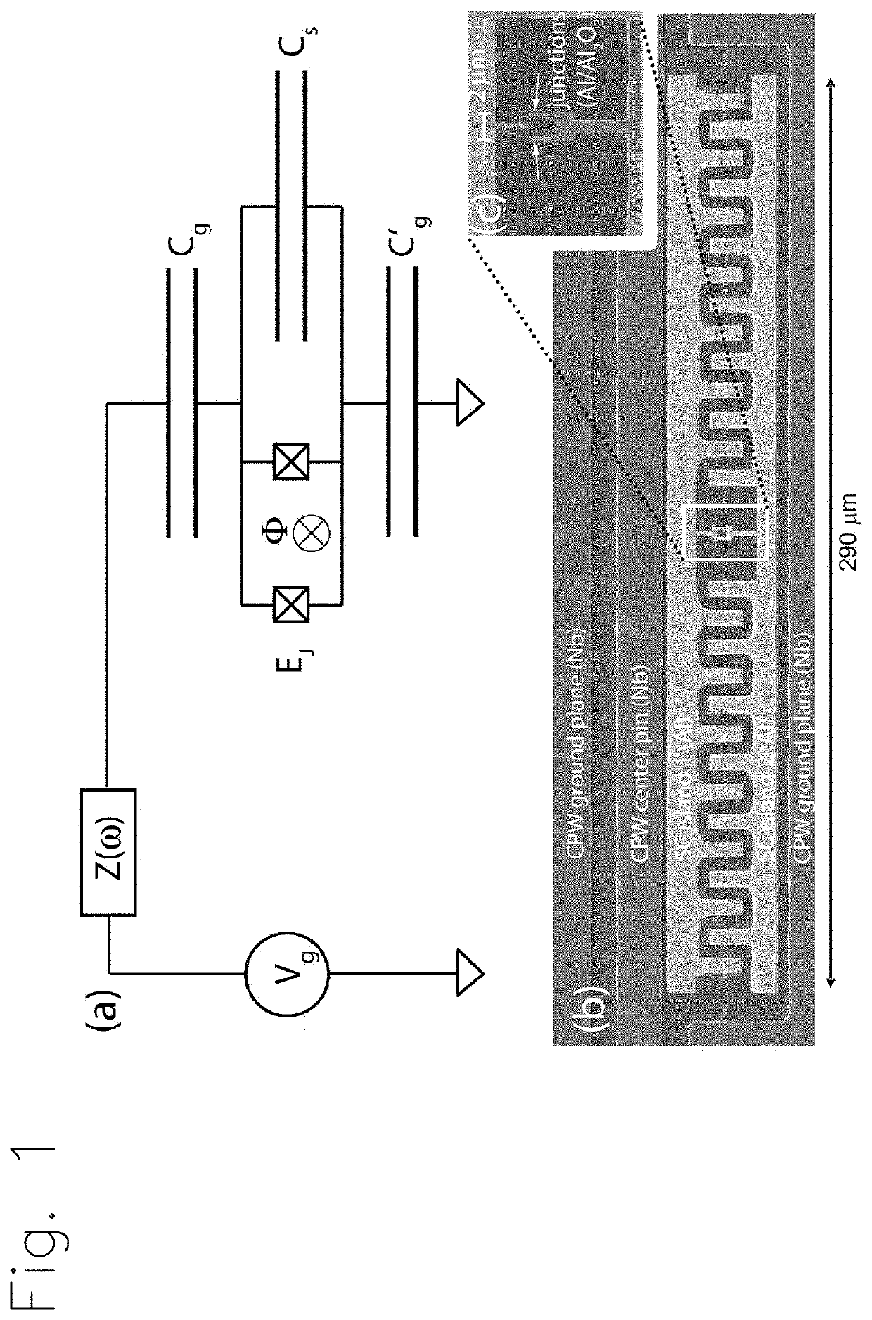
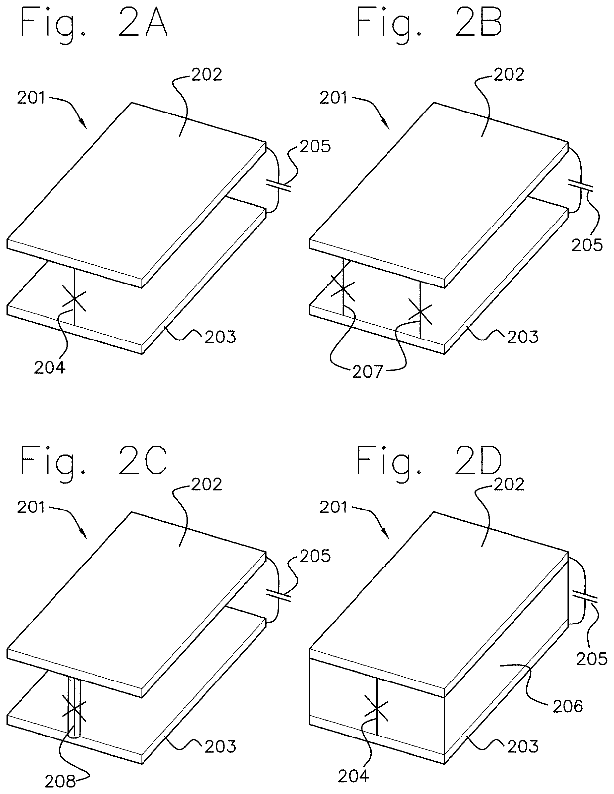
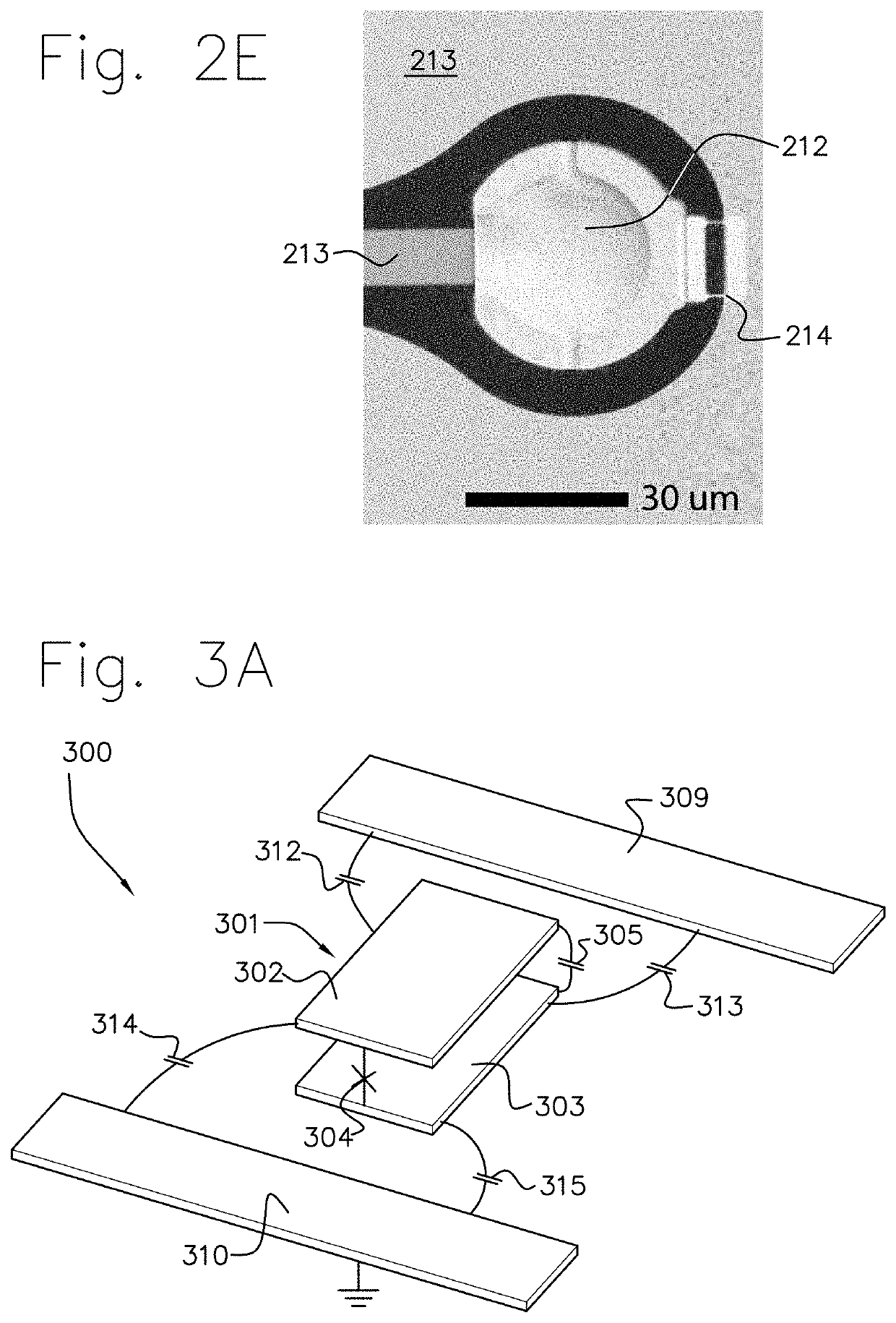
[0036]FIGS. 2A, 2B, 2C, 2D schematically show various transmon qubits according to the present invention. Here the transmon qubit is shown isolated without its connection to other circuit elements, such as transmission line resonators, control lines, the circuit ground. Therefore it is understood that the capacitive embedding of the transmon is omitted here.

[0037]FIG. 2A shows a transmon qubit according to an embodiment of the present invention. The transmon qubit 201 or the transmon qubit device comprises a plate capacitor comprising a first plate 202 and a second plate 203. The first plate 202 is disposed opposite to at least a part of the second plate 203. The first plate 202 and the second plate 203 are connected via a nonlinear inductance element 204. Furthermore, a capacitance 205 is formed between the first plate 202 and the second plate 203.

[0038]The first plate 202 can be disposed at a first layer, the second plate 203 can be disposed at a second layer which is not the firs...


PUM


Abstract

A transmon qubit comprising a plate capacitor comprising a first plate (202) and a second plate (203) wherein the first plate is disposed opposite to at least a part of the second plate, wherein the first plate and the second plate are connected via a nonlinear inductance element (304), and a capacitance (205) formed between the first plate and the second plate, wherein the first plate and the second plate are configured to form a vacuum gap capacitor.

Description

FIELD OF THE INVENTION[0001]The invention relates to a qubit apparatus and a qubit system, and more specifically, a transmon qubit and a transmon qubit system.BACKGROUND OF THE INVENTION[0002]A classical computer uses binary bits of 0 and 1 (on / off) to perform computational tasks. On the other hand a quantum computer uses the laws of quantum mechanics wherein a quantum bit can be both 0 and 1 simultaneously, using the quantum mechanical superposition principle. Such quantum processors allow to perform calculations beyond the capabilities of the best imaginable classical computers. A mayor engineering hurdle is the fact that the quantum information stored in the quantum state is very fragile to unwanted and uncontrolled environmental influences, known as decoherence. Performing quantum computation and quantum simulations on these processors require many classical control lines to manipulate, couple (entangle), transfer, and read out the quantum information stored in the quantum bit. ...

Claims


Application Information

Patent Timeline
IPC IPC(8): G11C11/44G06N10/00H01L39/22H01L39/02H01P7/08
CPCG06N10/00G11C11/44H01L39/025H01L39/223H01P7/08G06N10/40H10N60/12H10N60/805
Inventor BOSMAN, SAL JUASTEELE, GARY ALEXANDER
Owner TECH UNIV DELFT
Why Eureka
Try Eureka