Vertical channel organic thin-film transistor and manufacturing method thereof

a technology of organic thin-film transistors and manufacturing methods, applied in the field of display technology, can solve the problems of severe challenge in the control of precision of a manufacturing process, and achieve the effects of improving circuit design flexibility, increasing the scenarios of application of thin-film transistors, and reducing manufacturing difficulty and manufacturing costs

Inactive Publication Date: 2018-10-04
WUHAN CHINA STAR OPTOELECTRONICS TECH CO LTD
View PDF16 Cites 3 Cited by
  • Summary
  • Abstract
  • Description
  • Claims
  • Application Information

AI Technical Summary

Benefits of technology

[0006]Objectives of the present invention are to provide a vertical channel organic thin-film transistor, which reduces the difficulty and manufacturing cost of making a short channel pattern and saves a planar space of the thin-film transistor.
[0007]Objectives of the present invention are also to provide a manufacturing method of a vertical channel organic thin-film transistor, which reduces the difficulty and manufacturing cost of making a short channel pattern and saves a planar space of the thin-film transistor.
[0028]The efficacy of the present invention is that the present invention provides a vertical channel organic thin-film transistor, which comprises: an annular organic semiconductor layer, an annular drain electrode and an annular source electrode respectively set in contact with upper and lower sides of the annular organic semiconductor layer, and a gate electrode arranged inwardly of an inner circle of the annular organic semiconductor layer and insulated and isolated from the annular organic semiconductor layer, wherein an effective conductive channel length of the thin-film transistor can be varied by changing a thickness of the organic semiconductor layer made with a solution method so that the definition of a short channel pattern no longer relies upon high precision exposure and etching equipment and thus, the difficulty and the cost of the manufacturing process can be reduced. Further, the annular electrode structure makes it possible to save a planar space of the thin-film transistor, increasing scenarios of application of the thin-film transistor, and improving flexibility of circuit design. The present invention also provides a manufacturing method of a vertical channel organic thin-film transistor, which reduces manufacture difficulty and manufacturing cost of a short channel pattern and saves a planar space of the thin-film transistor.

Problems solved by technology

Thus, for a smaller length of the channel, the requirement for accuracy of vacuum equipment, particularly exposure and etching equipment, is severer, and particularly, when the channel design of thin-film transistors of an array contained in a display panel is one micrometer or less than one micrometer, control of precision of a manufacturing process would become a severe challenge.

Method used


Image

  • Vertical channel organic thin-film transistor and manufacturing method thereof
  • Vertical channel organic thin-film transistor and manufacturing method thereof
  • Vertical channel organic thin-film transistor and manufacturing method thereof

Examples


Embodiment Construction

[0042]To further expound the technical solution adopted in the present invention and the advantages thereof, a detailed description will be given with reference to the preferred embodiments of the present invention and the drawings thereof.

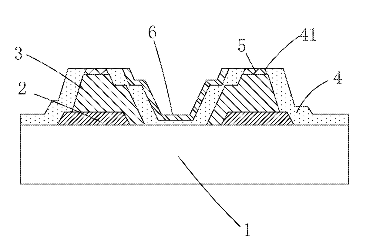
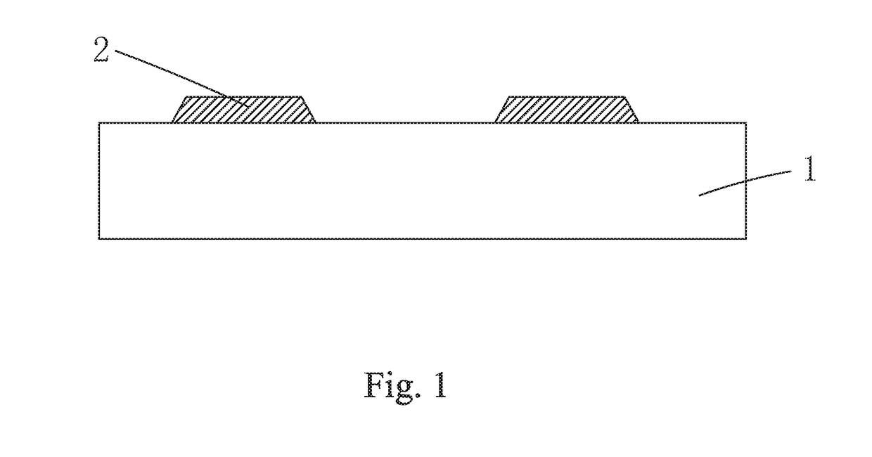
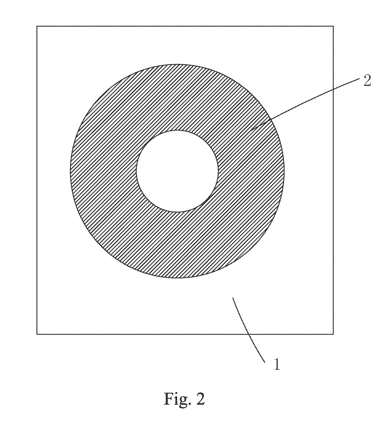
[0043]Referring to FIGS. 9 and 10, the present invention provides a vertical channel organic thin-film transistor, which comprises: a base plate 1, an annular source electrode 2 arranged on the base plate 1, an annular organic semiconductor layer 3 arranged on the source electrode 2 and a portion of the base plate 1 inwardly of an inner circle of the source electrode 2, an insulation layer 4 set on and covering the base plate 1, the source electrode 2, and the organic semiconductor layer 3, an annular via 41 extending through a portion of the insulation layer 4 located atop the organic semiconductor layer 3, an annular drain electrode 5 arranged in the annular via 41 and in contact with the organic semiconductor layer 3, and a gate electrode 6 arr...


PUM


Abstract

The present invention provides a vertical channel organic thin-film transistor and a manufacturing method thereof. The vertical channel organic thin-film transistor includes: an annular organic semiconductor layer, an annular drain electrode and an annular source electrode respectively set in contact with upper and lower sides of the annular organic semiconductor layer, and a gate electrode arranged inwardly of an inner circle of the annular organic semiconductor layer and insulated and isolated from the annular organic semiconductor layer. An effective conductive channel length of the thin-film transistor can be varied by changing a thickness of the organic semiconductor layer made with a solution method so that the definition of a short channel pattern no longer relies upon high precision exposure and etching equipment and thus, the difficulty and the cost of the manufacturing process can be reduced. Further, the annular electrode structure makes it possible to save a planar space of the thin-film transistor, increasing scenarios of application of the thin-film transistor, and improving flexibility of circuit design.

Description

BACKGROUND OF THE INVENTION1. Field of the Invention[0001]The present invention relates to the field of display technology, and more particular to a vertical channel organic thin-film transistor (TFT) and a manufacturing method thereof.2. The Related Arts[0002]With the development of the display technology, all sorts of flat panel display devices, including liquid crystal displays (LCDs) and organic light emitting displays (OLEDs), which show various advantages, such as high image quality, low power consumption, thin device body, and a wide range of applications, have been widely used in various consumer electronic products, such as mobile phones, televisions, personal digital assistants (PDAs), digital cameras, notebook computers, and desktop computers and are becoming a main stream of display devices.[0003]A thin-film transistor (TFT) is an electronic switching element that is commonly used in flat panel display devices and is generally constructed with a gate electrode, an active...

Claims


Application Information

Patent Timeline
Patent Type & Authority Applications(United States)
IPC IPC(8): H01L51/05H01L51/10H01L27/32
CPCH01L51/057H01L51/105H01L27/3274H10K10/491H10K10/84H10K59/125
Inventor LIU, ZHE
Owner WUHAN CHINA STAR OPTOELECTRONICS TECH CO LTD
Why Eureka
Try Eureka