Mask assembly and method for manufacturing the same and display device

a mask and assembly technology, applied in the field of display technologies, can solve the problems of poor alignment accuracy of the mask assembly, the evaporation region of the mask assembly cannot be effectively aligned the mask assembly cannot effectively align with the region of the substrate, so as to reduce the stress difference

Active Publication Date: 2018-07-26
BOE TECH GRP CO LTD +1
View PDF3 Cites 7 Cited by
  • Summary
  • Abstract
  • Description
  • Claims
  • Application Information

AI Technical Summary

Benefits of technology

This patent describes a design for a semiconductor device that reduces stress and improves reliability. It includes a buffer region and a peripheral region that are designed to minimize stress differences with the evaporation region, which helps prevent cracking and other damage. Additionally, the design includes the use of a second mask to form the buffer structures in the buffer region and peripheral region. Overall, this design improves the reliability and performance of semiconductor devices.

Problems solved by technology

However, since in the related art, the evaporation region of the mask assembly is defined by the opening region of the Open MASK, and the Open MASK will be easily deformed under a force during welding the FMM onto the Open MASK, relative positions of the opening region of the Open MASK and the metal frame will be changed, thereby the evaporation region of the mask assembly is changed, and the evaporation region of the mask assembly cannot be effectively aligned with the region of the substrate where the pattern is to be formed.
Thus, the mask assembly has a poorer alignment accuracy.

Method used


Image

  • Mask assembly and method for manufacturing the same and display device
  • Mask assembly and method for manufacturing the same and display device
  • Mask assembly and method for manufacturing the same and display device

Examples


Embodiment Construction

[0048]In order to make objects, technical schemes and advantages of the present disclosure more definite, the present disclosure will be described in detail hereinafter with reference to drawings. Obviously, the described embodiments are merely a part of embodiments of the present disclosure, rather than being all embodiments thereof. Based on the embodiments of the present disclosure, all other embodiments obtained by those ordinary skilled in the art without any inventive step will fall within the scope of the present disclosure.

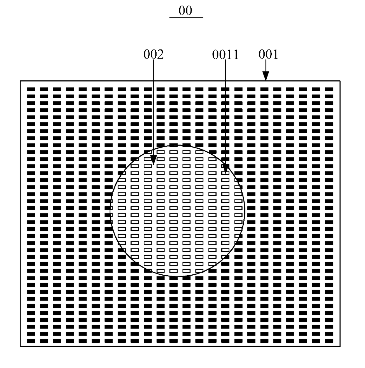
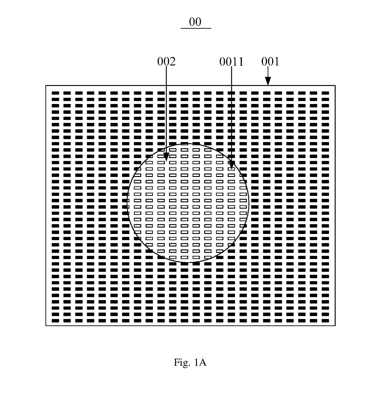
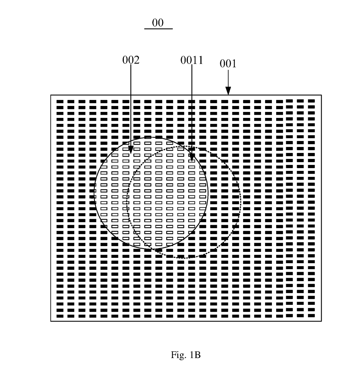
[0049]FIG. 1A is a structural schematic diagram showing a mask assembly 00 provided in related arts. Referring to FIG. 1A, the mask assembly 00 comprises a metal frame, an Open MASK and a FMM 001, the Open MASK comprises an opening region, the FMM 001 comprises evaporation holes 0011 precisely arranged in the whole FMM, the Open MASK and the FMM are welded at their peripheries onto the metal frame, the FMM 001 is superposed on the Open MASK, and among the ...


PUM

PropertyMeasurementUnit
stressaaaaaaaaaa
areasaaaaaaaaaa
areaaaaaaaaaaa

Abstract

The present disclosure provides a mask assembly and a method for manufacturing the same, and a display device. The mask assembly includes a frame, a first mask and a second mask, and the first mask and the second mask are superposed on the frame; the first mask includes an opening region, the second mask includes an evaporation region in which a first evaporation hole is provided for allowing an evaporation material to pass therethrough and a buffer region surrounding the evaporation region and configured to block off the evaporation material, and an orthographic projection of the boundary of the opening region onto the second mask is located within the buffer region.

Description

[0001]This application is the national phase of PCT Application No. PCT / CN2017 / 084717 filed on May 17, 2017, which in turn claims the benefit of Chinese Patent Application No. 201610423043.X filed on Jun. 15, 2016 in the State Intellectual Property Office of China, the whole disclosure of which is incorporated herein by reference.BACKGROUND OF THE DISCLOSUREField of the Disclosure[0002]Embodiments of the disclosure generally relate to the field of display technologies, and in particular to a mask assembly and a method for manufacturing the same, and a display device.Description of the Related Art[0003]Organic Light-Emitting Diode (OLED for short) display has advantages such as self-luminescence, a smaller thickness, a light weight, a fast response speed, a wide angle of view, rich colors, a high brightness, a low power consumption, resistance to high and low temperature and the like, and is widely applied in products such as a mobile phone, a watch, a computer, a TV set and the like...

Claims


Application Information

Patent Timeline
Patent Type & Authority Applications(United States)
IPC IPC(8): C23C14/04C23C14/24H01L27/32
CPCC23C14/04C23C14/24H01L27/3223C23C14/042H10K59/00H10K59/88
Inventor LI, DONGWEILI, BAOJUNHUANG, CHUN CHIEH
Owner BOE TECH GRP CO LTD
Why Eureka
Try Eureka