
Display panel and thin film transistor array substrate

a technology of thin film transistors and display panels, applied in the field of displays, can solve the problems of short-circuit problems and affect the touch control of the display panel, and achieve the effect of avoiding metal remaining

Active Publication Date: 2018-06-21
WUHAN CHINA STAR OPTOELECTRONICS TECH CO LTD
View PDF1 Cites 3 Cited by
  • Summary
  • Abstract
  • Description
  • Claims
  • Application Information

AI Technical Summary

Benefits of technology

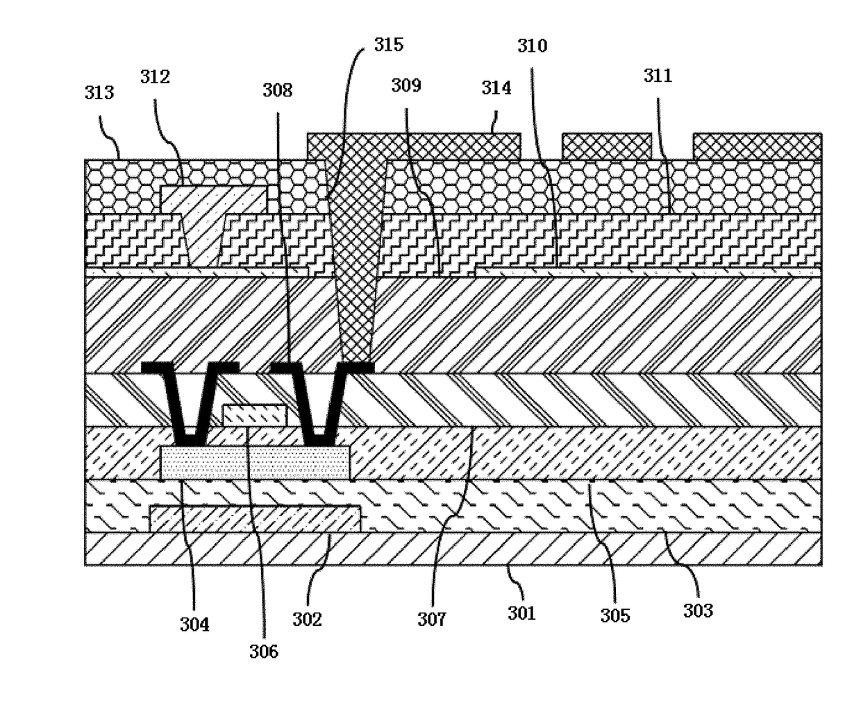
The present invention aims to provide a display panel and its driving method that avoids metal remaining in the trench region and prevents wires from short-circuiting. This is achieved by designing a liquid crystal display panel and thin film transistor array substrate that eliminates residual metal in the edge of the groove of the third insulating layer. The invention prevents wire shorts caused by residual metal and ensures a better fan-out area for the wires.

Problems solved by technology

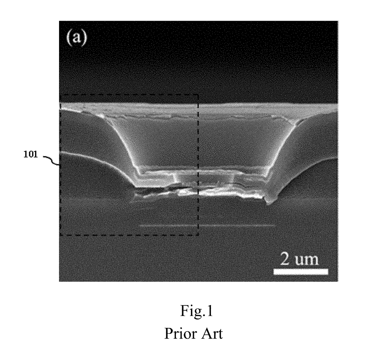
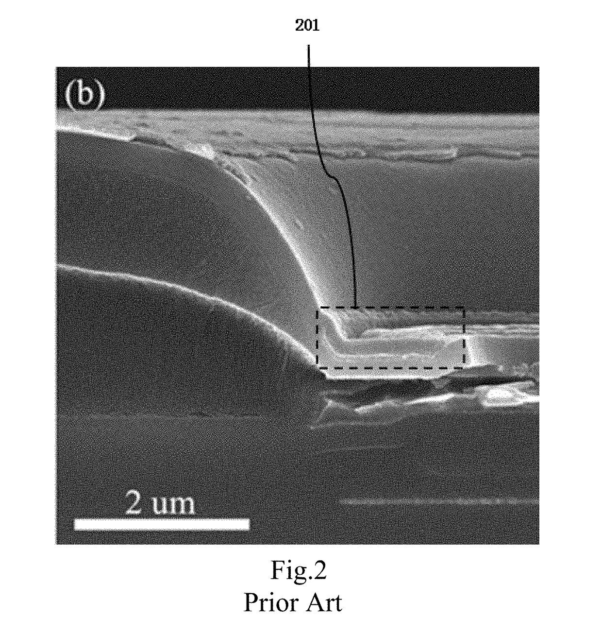
Refer to FIGS. 1 and 2, some residual metal is left in the touch-sensing line layer, so that the fan-out wires will have a short-circuit problem, and the touch control of the display panel will be affected.

Method used


Image

  • Display panel and thin film transistor array substrate
  • Display panel and thin film transistor array substrate
  • Display panel and thin film transistor array substrate

Examples


Embodiment Construction

[0032]Regarding the words used in the present specification, “an embodiment” means used as an example, examples, or illustrations. In addition, in this specification and the appended claims the article “a” in general can be interpreted to mean “one or more” unless specified otherwise or clear from the context to be oriented to the singular form.

[0033]A display panel according to a preferred embodiment of the present invention is a thin film transistor liquid crystal display. The display panel has a color filter substrate, a liquid crystal layer, and a thin film transistor array substrate. The color filter substrate and the thin film transistor array substrate are assembled as one piece, and the liquid crystal layer is disposed between the color filter substrate and the thin film transistor array substrate.

[0034]Refer to FIG. 3, which is a cross-sectional view of a display area of a thin film transistor array substrate according to the present invention. The thin film transistor arra...


PUM

PropertyMeasurementUnit
temperatureaaaaaaaaaa
areaaaaaaaaaaa
display areaaaaaaaaaaa

Abstract

A liquid crystal display panel and a thin film transistor array substrate are provided. The thin film transistor array substrate includes a pixel area and a fan-out area. The fan-out area has a groove. The thin film transistor array substrate has a substrate, a light shielding layer, a buffer layer, a poly-silicon layer, a first insulating layer, a scan line layer, a second insulating layer, a data line layer, a third insulating layer, a common line layer, a touch-sensing line layer, a fourth insulating layer, and a pixel electrode layer. The present invention can prevent wire shorts.

Description

FIELD OF THE INVENTION[0001]The present invention relates to a technical field of displays, and in particular to a liquid crystal display panel and a thin film transistor array substrate.BACKGROUND OF THE INVENTION[0002]The traditional display panel, such as a low temperature poly-silicon liquid crystal display (LTPS-LCD), fan-out wires are disposed by using the touch-sensing line layer (M3). In a manufacturing process of the display panel, the planarization layer is thicker, and the photoresist easily remains in the trench region of the planarization layer after exposure. Refer to FIGS. 1 and 2, some residual metal is left in the touch-sensing line layer, so that the fan-out wires will have a short-circuit problem, and the touch control of the display panel will be affected.[0003]Therefore, a liquid crystal display panel and a thin film transistor array substrate needs to be developed which can solve the problems existing in the conventional art described above.SUMMARY OF THE INVEN...

Claims


Application Information

Patent Timeline
Patent Type & Authority Applications(United States)
IPC IPC(8): G02F1/1362G02F1/1333G02F1/1368G02F1/1335G06F3/041G09G3/36
CPCG02F1/136286G02F1/13338G02F1/1368G02F1/133514G02F1/133345G06F3/0412G09G3/36G02F2202/104G02F2201/123G02F1/136227H01L27/124G02F1/1345G06F2203/04103G06F3/04164G02F1/134372
Inventor CHEN, GUIXUE, JINGFENG
Owner WUHAN CHINA STAR OPTOELECTRONICS TECH CO LTD
Learn More