Optical signal processing device
a signal processing and optical technology, applied in optics, instruments, electrical equipment, etc., can solve the problems of increasing loss, multicast switching inherently producing theoretical loss, and limit of multicast switching, so as to increase the number of aggregated transponders without increasing theoretical loss
- Summary
- Abstract
- Description
- Claims
- Application Information
AI Technical Summary
Benefits of technology
Problems solved by technology
Method used
Image
Examples
embodiment 1
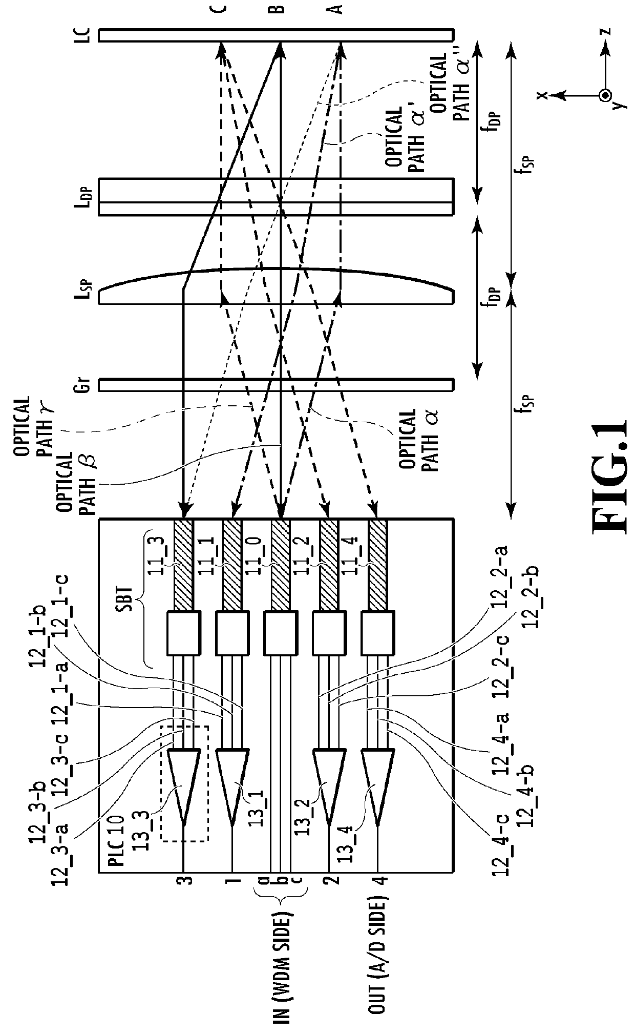
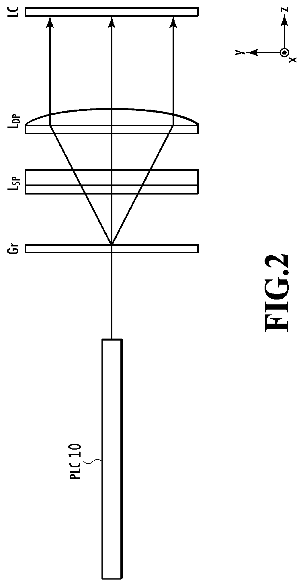
[0032]FIGS. 1 and 2 each show an outline of the configuration of an optical signal processing device according to Embodiment 1 of the present invention. FIG. 1 is a top view seen in the y-axis direction, and FIG. 2 is a side view seen in the x-axis direction. Throughout the drawings used in the following description of the present invention, the same components are denoted by the same reference signs. In the present embodiment, M×N wavelength selective switch of M×N=3×4 is used as an example, where M is the number of inputs and N is the number of outputs. However, the numbers of inputs and outputs are obviously not limited to this example.
[0033]In FIG. 1, optical signals inputted from input ports a, b, and c denoted as IN (WDM SIDE) (M=3 in this embodiment) are inputted to a planar lightwave circuit (PLC) 10.
[0034]PLC 10 has spatial beam transformers (SBTs) 11_0 to 11_4 (see NPL 3), and the input ports a, b, and c are connected to the input-end SBT 11_0.
[0035]The SBTs 11_0 to 11_4 a...
embodiment 2
[0056]FIG. 4 shows the configuration of a multiplex part of an optical signal processing device according to Embodiment 3 of the present invention. As in Embodiment 1, FIG. 4 is a cutout of the part in FIG. 1 framed by the dotted line. Conditions such as the number of ports are the same as those in Embodiment 1.
[0057]FIG. 4 shows an example of the configuration of the multiplex part in which a part which is formed by a 1×2 optical coupler in Embodiment 1 is formed by an optical switch using a Mach-Zehnder interferometer (MZI).
[0058]MZI optical switches 151, 152, and 153 are each formed by two 2×2 couplers, two arm waveguides between the 2×2 couplers, and a control heater 161, 162, or 163 disposed immediately above one or both of the arm waveguides. When power is applied to the control heater, the phase of light propagating immediately below the control heater is changed due to thermooptical effect, and switch is made between a cross state and a bar state. Thereby, for instance, a si...
embodiment 3
[0063]FIG. 5 shows the configuration of a multiplex part of an optical signal processing device according to Embodiment 3 of the present invention. In this embodiment, only the stage of the multiplex part 13_j close to the intermediate output waveguide 12_j is configured with MZI optical switches, and the output-port side is configured with a 1×2 optical coupler. Specifically, one of the outputs of the MZI optical switch 152 and one of the outputs of the MZI optical switch 153 are connected to the two input ports of one 1×2 optical coupler 141. To apply this configuration to the multiplex part 13_j of Embodiment 1, the input ports 13_j-a, 13_j-b, and 13_j-c may be used to configure an M=3 multiplex part 13_j.
[0064]Advantages of this configuration are that: (1) the circuit size is not increased, (2) crosstalk of same-wavelength signals described in Embodiment 2 can be reduced, and (3) theoretical loss can be reduced more than Embodiment 1. For example, crosstalk of wavelength is the...
PUM
 Abstract
Description
Claims
Application Information
 - R&D
- Intellectual Property
- Life Sciences
- Materials
- Tech Scout
- Unparalleled Data Quality
- Higher Quality Content
- 60% Fewer Hallucinations
Browse by: Latest US Patents, China's latest patents, Technical Efficacy Thesaurus, Application Domain, Technology Topic, Popular Technical Reports.
© 2025 PatSnap. All rights reserved.Legal|Privacy policy|Modern Slavery Act Transparency Statement|Sitemap|About US| Contact US: help@patsnap.com


