Gas injector device used for semiconductor equipment
- Summary
- Abstract
- Description
- Claims
- Application Information
AI Technical Summary
Benefits of technology
Problems solved by technology
Method used
Image
Examples
Embodiment Construction
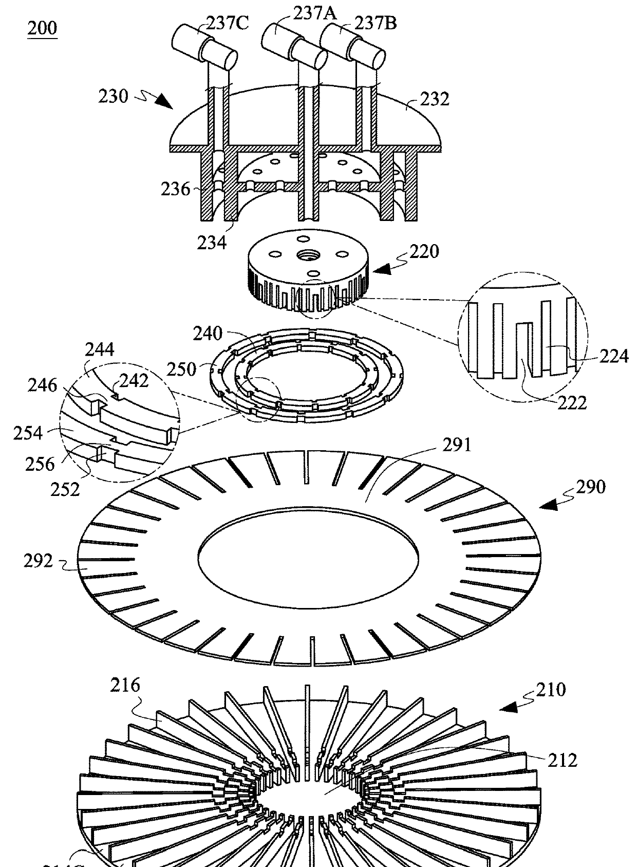
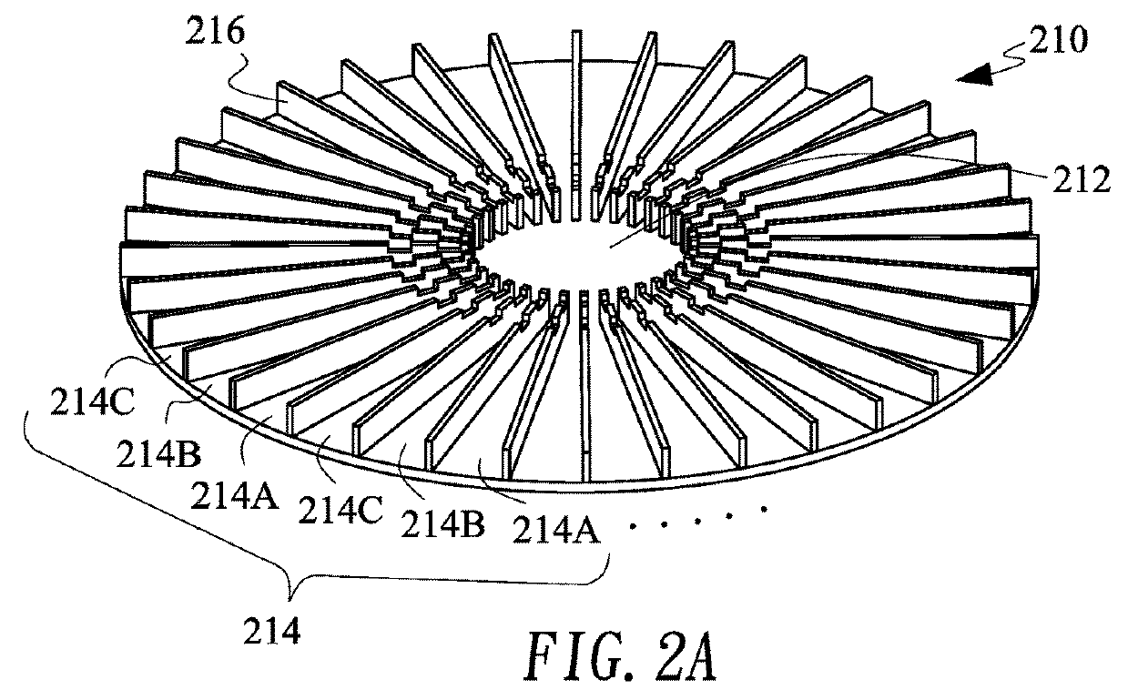
[0023]FIG. 2A shows an exploded view of a gas injector 200 adaptable to semiconductor equipment according to one embodiment of the present invention, and FIG. 2B shows a partial cross-sectional view of the gas injector 200 of FIG. 2A. The gas injector 200 of the embodiment may include a base plate 210, a center sleeve cover 220, an intake body 230, an inner cover 240 and an outer cover 250. The base plate 210 has a central zone 212 and a plurality of channels 214. The channels 214, surrounding the central zone 212, are disposed on the base plate 210 in sequence. The channels 214 may include first channels 214A, second channels 214B and third channels 214C. The center sleeve cover 220 is disposed in the central zone 212, and is operatively coupled with the base plate 210 to form a first cavity 260A.
[0024]Specifically, a wall of the center sleeve cover 220 joins inner ends of the channels 214, and has a plurality of first communicating openings 222 correspondingly connected to the fir...
PUM
| Property | Measurement | Unit |
|---|---|---|
| Thickness | aaaaa | aaaaa |
| Size | aaaaa | aaaaa |
Abstract
Description
Claims
Application Information
 - R&D
- Intellectual Property
- Life Sciences
- Materials
- Tech Scout
- Unparalleled Data Quality
- Higher Quality Content
- 60% Fewer Hallucinations
Browse by: Latest US Patents, China's latest patents, Technical Efficacy Thesaurus, Application Domain, Technology Topic, Popular Technical Reports.
© 2025 PatSnap. All rights reserved.Legal|Privacy policy|Modern Slavery Act Transparency Statement|Sitemap|About US| Contact US: help@patsnap.com


