
Display Device and Method of Manufacturing the Same

a technology of light-emitting display device and display device, which is applied in the direction of solid-state device, semiconductor device, organic semiconductor device, etc., can solve the problems of low manufacturing cost, light-emitting display device, fast response time, etc., and achieve the effect of reducing the consumption power of organic light-emitting display device, reducing the loss of light emitted, and increasing the lifetime of organic light-emitting devi

Active Publication Date: 2017-10-12
LG DISPLAY CO LTD
View PDF2 Cites 24 Cited by
  • Summary
  • Abstract
  • Description
  • Claims
  • Application Information

AI Technical Summary

Benefits of technology

The patent describes a new method for making organic light emitting displays that reduces the amount of light that is lost from the display. This method also increases the lifespan of the display and decreases the amount of power consumed by it.

Problems solved by technology

Furthermore, the organic light emitting display devices are driven with a low direct current (DC) voltage, have a fast response time, and are low in manufacturing cost.
However, even in a top emission type OLED display, when the light emitted from the organic light emitting device travels in a direction toward a bank dividing the organic light emitting device, instead of the direction toward the upper substrate, the light can be lost without being irradiated in the direction toward the upper substrate.

Method used


Image

  • Display Device and Method of Manufacturing the Same
  • Display Device and Method of Manufacturing the Same
  • Display Device and Method of Manufacturing the Same

Examples


Embodiment Construction

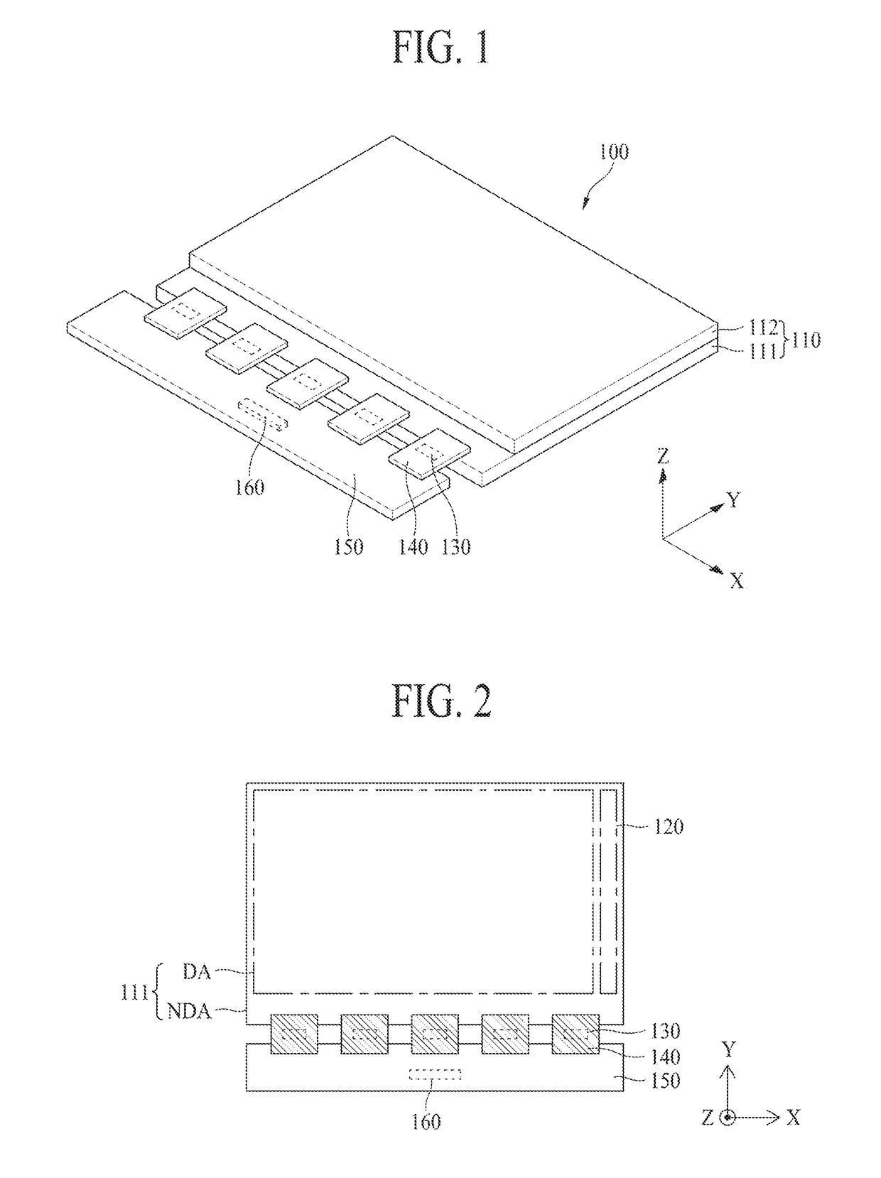
[0035]Reference will now be made in detail to the exemplary embodiments of the present invention, examples of which are illustrated in the accompanying drawings. Wherever possible, the same reference numbers will be used throughout the drawings to refer to the same or like parts.

[0036]Advantages and features of the present invention, and implementation methods thereof will be clarified through following embodiments described with reference to the accompanying drawings. The present invention may, however, be embodied in different forms and should not be construed as limited to the embodiments set forth herein. Rather, these embodiments are provided so that this disclosure will be thorough and complete, and will fully convey the scope of the present invention to those skilled in the art. Further, the present invention is only defined by scopes of claims.

[0037]A shape, a size, a ratio, an angle, and a number disclosed in the drawings for describing embodiments of the present invention ...


PUM


Abstract

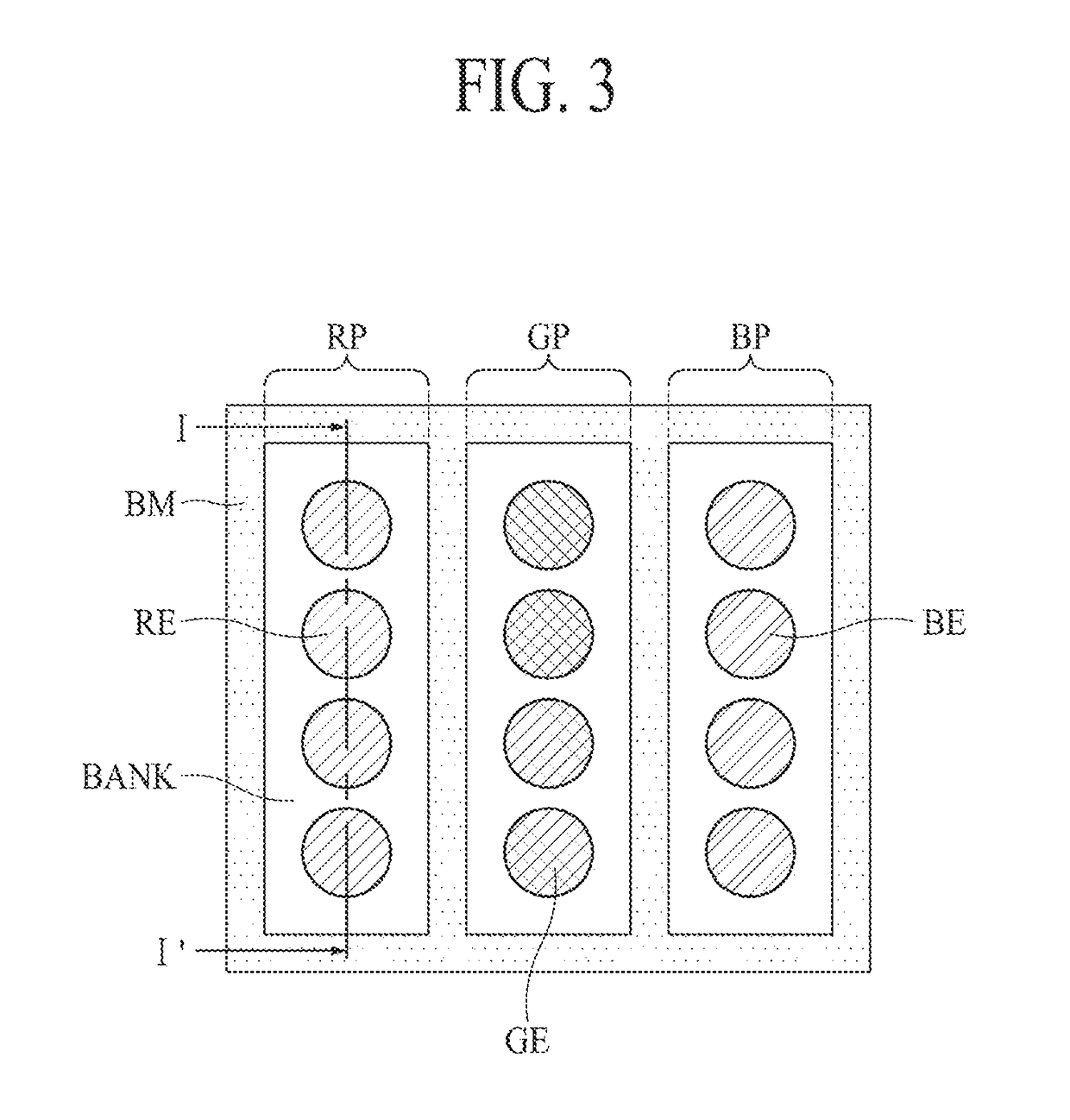
Disclosed are an organic light emitting display device and a method of manufacturing the same, which reduce a loss of light emitted from an organic light emitting device, increase a lifetime of the organic light emitting device, and decrease consumption power of the organic light emitting display device. The organic light emitting display device includes a first electrode disposed on a first substrate, a bank disposed on the first electrode for dividing a plurality of emission parts, an organic light emitting layer disposed on the first electrode and the bank, a second electrode disposed on the organic light emitting layer, and an encapsulation layer disposed on the second electrode. The encapsulation layer fills a space between adjacent banks, and a refractive index of the bank is lower than a refractive index of the organic light emitting layer and a refractive index of the encapsulation layer.

Description

CROSS-REFERENCE TO RELATED APPLICATIONS[0001]This application claims the benefit of the Korean Patent Application No. 10-2016-0044115 filed on Apr. 11, 2016, which is hereby incorporated by reference as if fully set forth herein.BACKGROUNDField of the Invention[0002]The present invention relates to an organic light emitting display device and a method of manufacturing the same.Discussion of the Related Art[0003]With the advancement of information-oriented society, various requirements for display devices for displaying an image are increasing. Therefore, various display devices such as liquid crystal display (LCD) devices, plasma display panel (PDP) devices, organic light emitting display devices, etc. are being used recently.[0004]As a type of display device, organic light emitting diode (OLED) display devices are self-emitting display devices and are better in viewing angle and contrast ratio than LCD devices. Also, since the organic light emitting display devices do not need a se...

Claims


Application Information

Patent Timeline
IPC IPC(8): H01L27/32H01L51/56H01L51/52
CPCH01L27/3246H01L51/5253H01L27/3258H01L2227/323H01L51/5275H01L51/56H01L27/3262H10K59/353H10K59/124H10K59/122H10K59/8731H10K59/80515H10K59/879H10K2102/3026H10K59/873H10K59/878H10K50/11H10K59/1201H10K71/821H10K50/813H10K50/844H10K50/858H10K59/1213H10K71/00
Inventor YOO, DONGHEEPARK, TAEHANLEE, KYUNGHOON
Owner LG DISPLAY CO LTD
Learn More