
Custom layout of integrated circuit (IC) designs

a technology of integrated circuits and designs, applied in the field of custom layout of integrated circuit designs, can solve the problems of increasing the difficulty of shrinking device sizes, becoming very difficult, if not impossible, and optimizing both performance and power at these process nodes, and achieve the effect of facilitating custom layout of multi-gate devices

Active Publication Date: 2017-10-05
SYNOPSYS INC
View PDF44 Cites 10 Cited by
  • Summary
  • Abstract
  • Description
  • Claims
  • Application Information

AI Technical Summary

Benefits of technology

The patent describes a tool for creating and manipulating IC design layouts that include multigate devices, such as FinFET devices. The tool has graphical user interface features that make it easy to customize the placement of these devices. The tool can also assign different colors to different parts of the design to help users connect them correctly. Additionally, the tool can create electrical contacts and cut shapes in the design layout. The "technical effect" of this patent is to provide a more efficient and effective tool for designing complex IC devices that include multigate devices.

Problems solved by technology

However, as process technologies approach and move past the 20-nanometers (nm) process node, it is becoming increasingly difficult to shrink device sizes.
Specifically, it has become very difficult, if not impossible, to optimize both performance and power at these process nodes.
However, this means that the drive strength of each “fin” is also low.
One approach is to increase the height of the “fin.” However, reliably manufacturing FinFETs with different fin heights can be very challenging.
It can be very time-consuming and cumbersome to use conventional IC design tools to create and manipulate IC design layouts, especially those that include multigate devices, such as FinFET devices.

Method used


Image

  • Custom layout of integrated circuit (IC) designs
  • Custom layout of integrated circuit (IC) designs
  • Custom layout of integrated circuit (IC) designs

Examples


Embodiment Construction

[0026]The following description is presented to enable any person skilled in the art to make and use the invention, and is provided in the context of a particular application and its requirements. Various modifications to the disclosed embodiments will be readily apparent to those skilled in the art, and the general principles defined herein may be applied to other embodiments and applications without departing from the spirit and scope of the present invention. Thus, the present invention is not limited to the embodiments shown, but is to be accorded the widest scope consistent with the principles and features disclosed herein.

Overview of IC Design

[0027]IC design software tools can be used to create an IC design. Once the IC design is finalized, it can undergo fabrication, packaging, and assembly to produce IC chips. The overall IC design and manufacturing process can involve multiple entities, e.g., one company may create a software tool that is used in the IC design flow, another...


PUM


Abstract

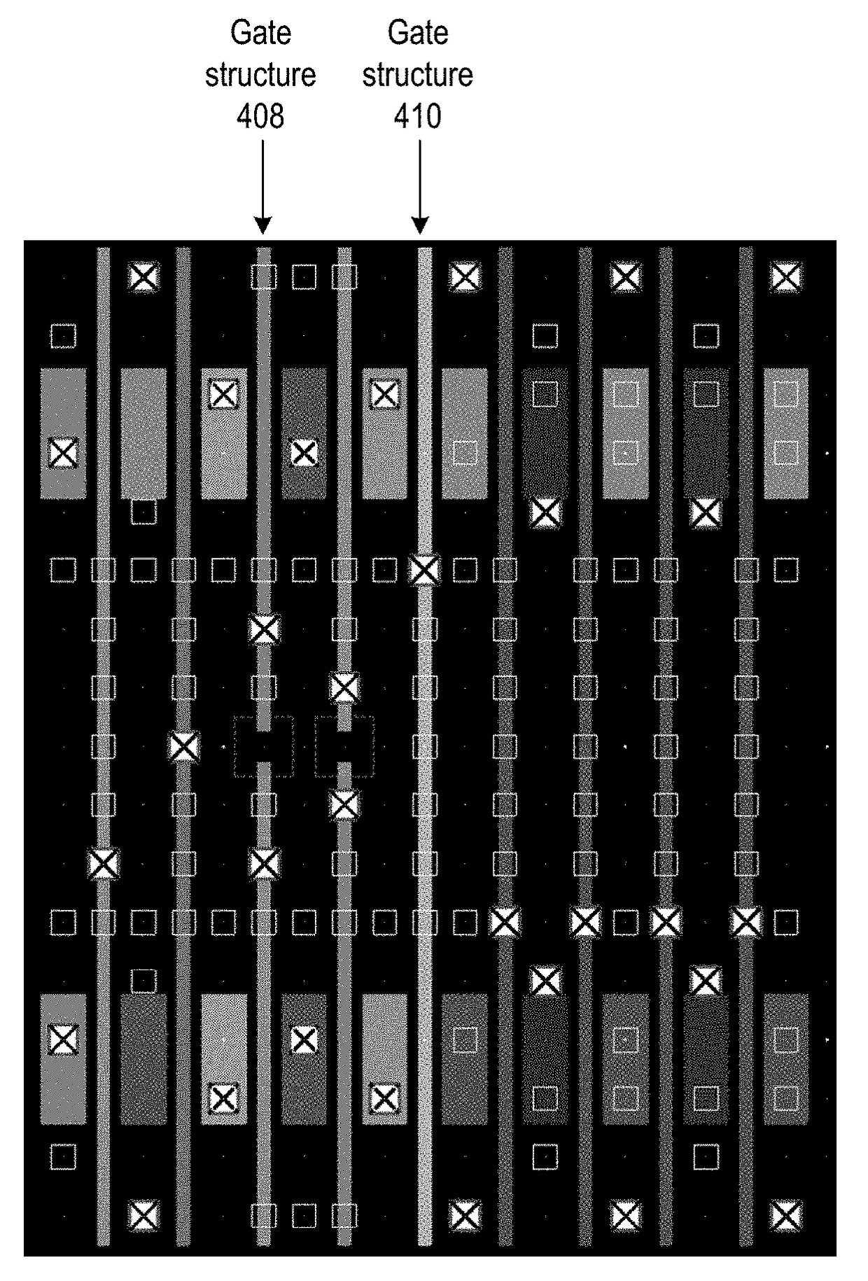
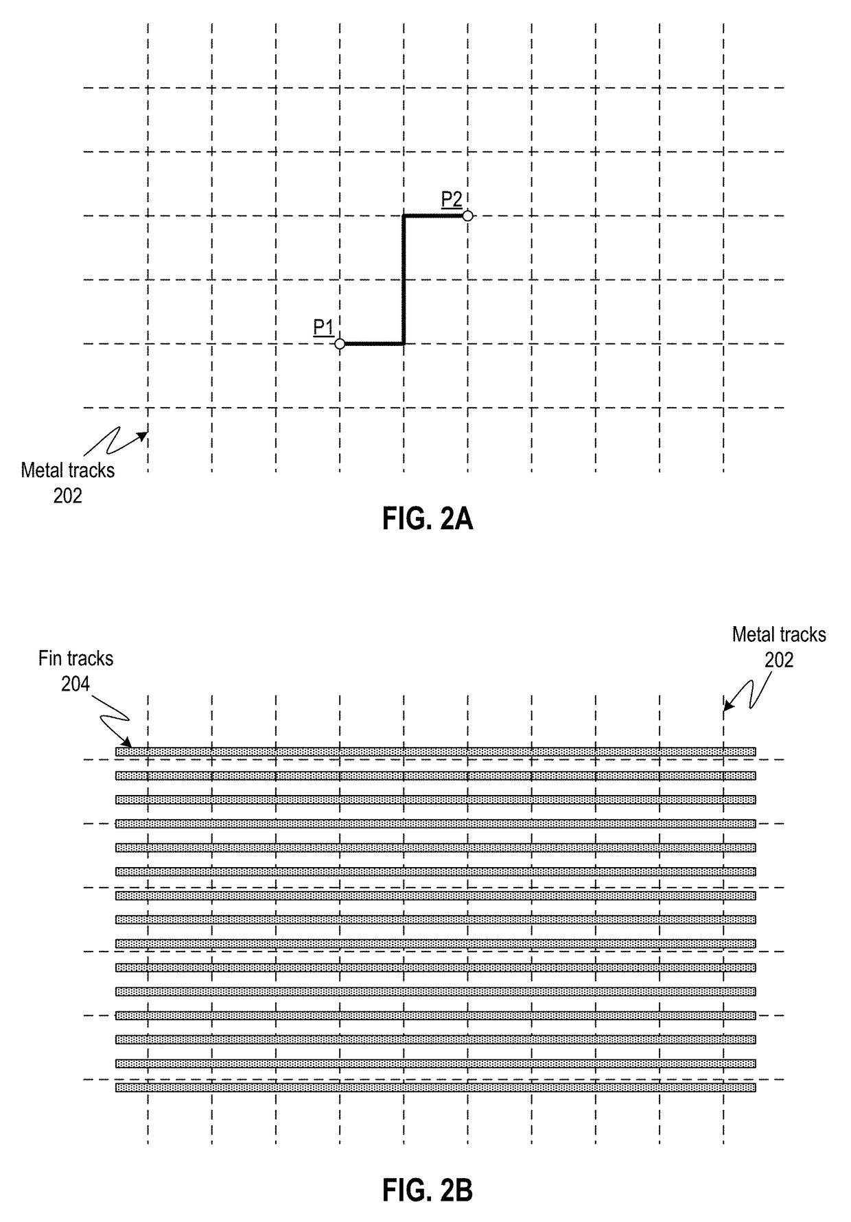
Systems and techniques for facilitating layout of an integrated circuit (IC) design are described. A distinct color pattern can be assigned to a set of shapes in a layout of the IC design that correspond to a net. Next, the layout of the IC design can be displayed in a graphical user interface (GUI) of the IC design tool. Some embodiments can move a diffusion region of a multigate device with respect to the location of the device contacts so that the diffusion region is aligned with respect to a set of fin tracks, wherein each fin of each multigate device is located on a fin track.

Description

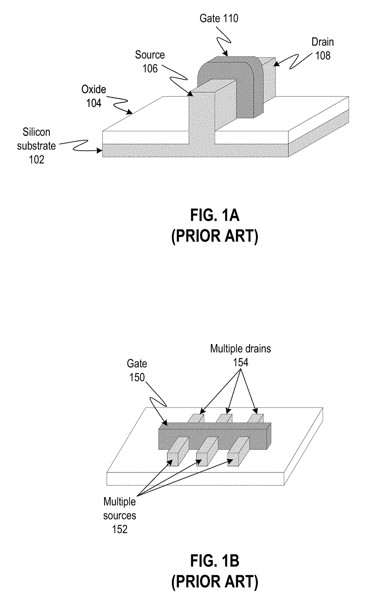
TECHNICAL FIELD[0001]This disclosure relates to integrated circuit (IC) design. More specifically, this disclosure relates to custom layout of IC designs.BACKGROUNDRelated Art[0002]Improvements in process technologies and IC design software tools have continued to shrink device sizes for decades. However, as process technologies approach and move past the 20-nanometers (nm) process node, it is becoming increasingly difficult to shrink device sizes. Specifically, it has become very difficult, if not impossible, to optimize both performance and power at these process nodes.[0003]Three-dimensional (3D) multigate device designs (FinFET technology being one such multigate technology) promise to continue the relentless march toward smaller device sizes. In particular, these 3D multigate device designs allow optimization of both performance and power when compared to traditional planar device designs.[0004]FIG. 1A illustrates a FinFET device. A FinFET device has a three-dimensional structu...

Claims


Application Information

Patent Timeline
IPC IPC(8): G06F17/50
CPCG06F17/5072H01L27/0886G06F17/5077G06F2111/20G06F30/392G06F30/398G06F30/394G06F30/31G06F2111/16
Inventor LEFFERTS, ROBERT B.
Owner SYNOPSYS INC
Learn More