
Display device and method of manufacturing a display device

Active Publication Date: 2017-06-29
JAPAN DISPLAY INC
View PDF3 Cites 2 Cited by
  • Summary
  • Abstract
  • Description
  • Claims
  • Application Information

AI Technical Summary

Benefits of technology

The technical effect of this patent is to provide a display device that stops neighboring pixels from mixing colors and avoids voltage drops caused by dividing the common electrode.

Problems solved by technology

As a result, there is a possibility that the above-mentioned color mixing may occur.

Method used


Image

  • Display device and method of manufacturing a display device
  • Display device and method of manufacturing a display device
  • Display device and method of manufacturing a display device

Examples


Embodiment Construction

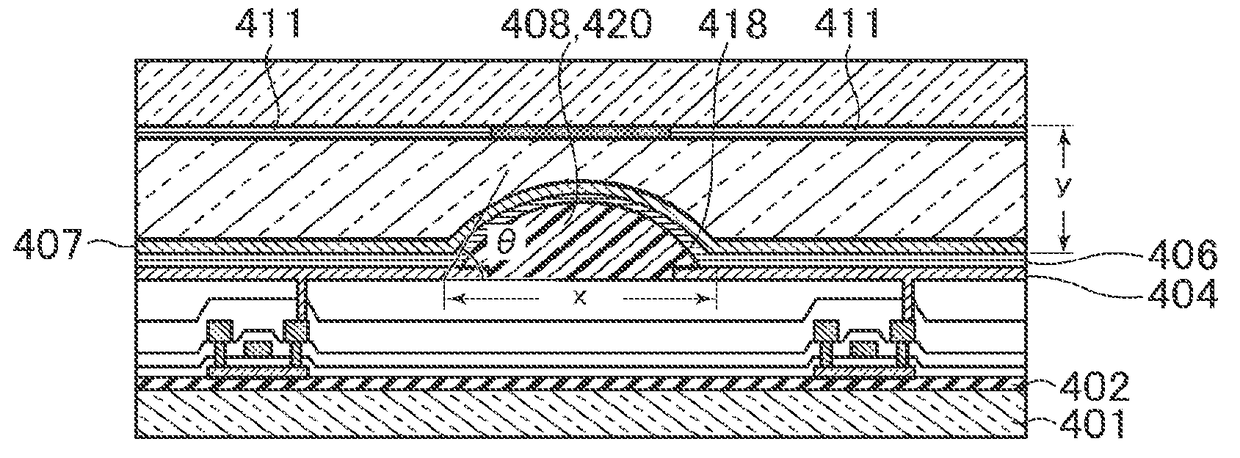
[0037]Embodiments of the present invention are described below with reference to the attached drawings. The disclosure is only exemplary, and modifications made as appropriate within the gist of the present invention that can be conceived with ease by those skilled in the art are naturally within the scope of the present invention. For clearer illustration, some widths, thicknesses, shapes, and the like of respective portions are schematically illustrated in the drawings in comparison to actual ones. However, the widths, the thicknesses, the shapes, and the like are merely an example, and do not limit understanding of the present invention. Further, like elements as those described relating to the drawings already referred to be denoted by like reference symbols herein and in each of the drawings, and detailed description thereof is sometimes omitted as appropriate.

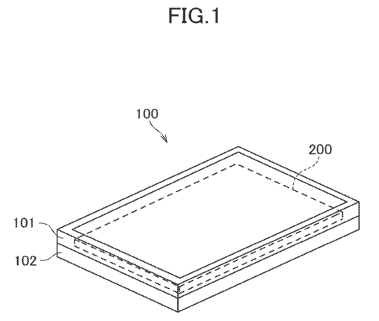
[0038]FIG. 1 is a view for schematically illustrating a display device 100 according to an embodiment of the present in...


PUM


Abstract

A display device, which includes a plurality of unit pixels, includes a plurality of first electrodes respectively corresponding to the plurality of unit pixels, an insulating layer which includes a plurality of through holes, a light emitting element layer, and a second electrode. Each of the plurality of through holes have inner surfaces including a forwardly tapered surface, which is inclined in a direction of enlarging the apertures toward a light emitting direction, and a reversely tapered surface, which is inclined in a direction of reducing the apertures toward the light emitting direction. The forwardly tapered surface is formed between the unit pixels arranged side by side in the first direction. The reversely tapered surface is formed between the unit pixels arranged side by side in the second direction.

Description

CROSS-REFERENCE TO RELATED APPLICATION[0001]The present application claims priority from the Japanese Application JP 2015-255388 filed on Dec. 25, 2015, the content of which is hereby incorporated by reference into this application.BACKGROUND OF THE INVENTION[0002]1. Field of the Invention[0003]The present invention relates to a display device and a method of manufacturing a display device.[0004]2. Description of the Related Art[0005]In recent years, needs for slim display devices have been increased along with informatization development. Slim display devices such as liquid crystal display devices, plasma displays, and organic electro-luminescent (EL) display devices have been put into practical uses. In addition, research and development for increasing resolution and display quality and for reducing manufacturing cost of each type of slim display devices has been actively conducted.[0006]According to Japanese Patent Application Laid-open No. 2014-179163, for example, there is disc...

Claims


Application Information

Patent Timeline
IPC IPC(8): H01L27/32H01L51/56H01L51/52
CPCH01L27/3246H01L27/3272H01L2227/323H01L51/5225H01L51/56H01L27/322H10K59/35H10K59/38H10K59/122H10K50/822H10K50/865H10K59/1201H10K71/00H10K2102/351H10K59/126
Inventor MATSUMOTO, YUKIO
Owner JAPAN DISPLAY INC
Learn More