
Device for incoupling and/or outcoupling optical signals

a technology of optical signals and incoupling devices, applied in the direction of optics, instruments, optical light guides, etc., can solve the problems of increased manufacturing costs, increased optical loss, and increased optical loss, so as to achieve low optical loss and low manufacturing costs

Active Publication Date: 2017-03-16
SILICON LINE
View PDF4 Cites 0 Cited by
  • Summary
  • Abstract
  • Description
  • Claims
  • Application Information

AI Technical Summary

Benefits of technology

The present invention is aimed at improving coupling and decoupling devices of the type described earlier. The goal is to make the devices more efficient and easy to manufacture, without requiring precise alignment of the waveguide. Additionally, the invention aims to minimize the size of the devices while maintaining low optical losses. The stated goal is to make the coupling and decoupling devices more user-friendly and cost-effective.

Problems solved by technology

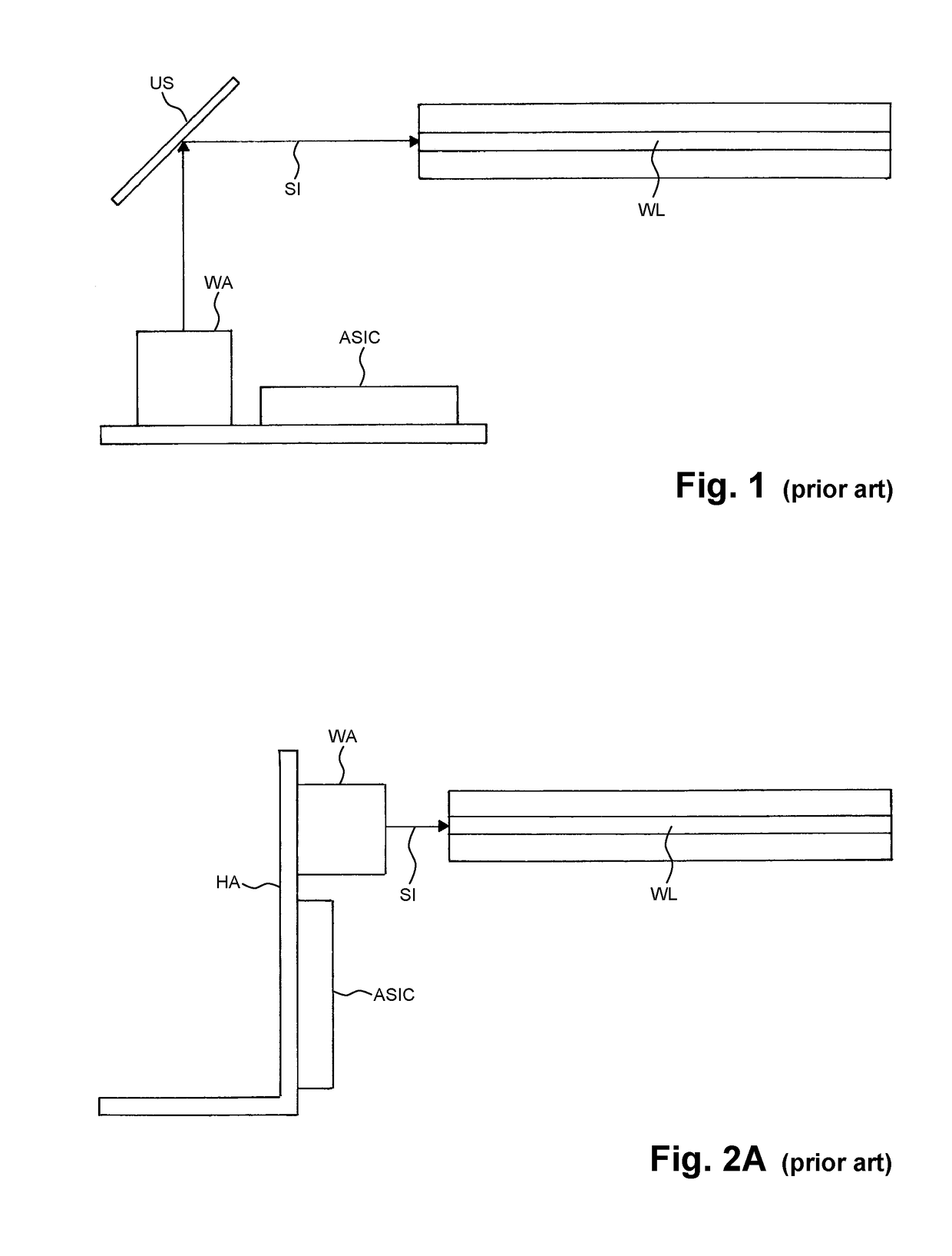
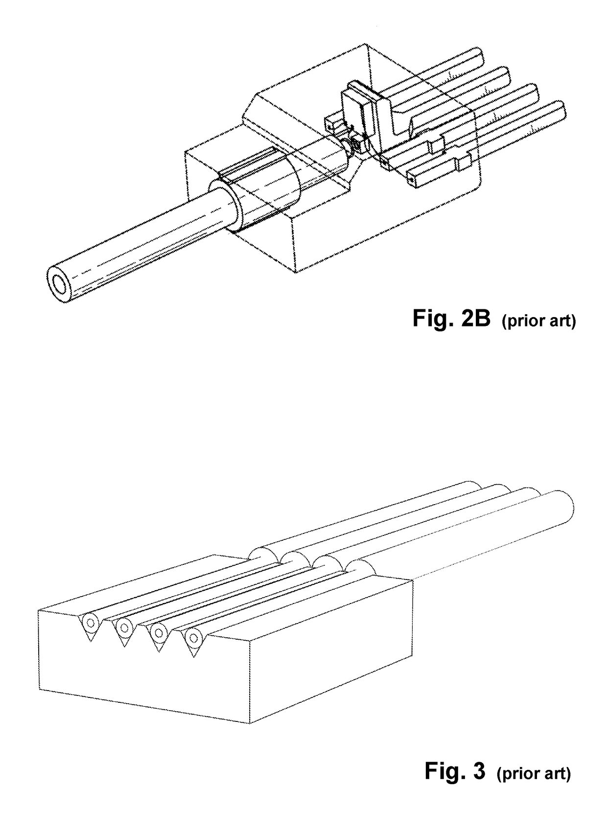
The disadvantage to the solutions known from prior art consists in that the alignment of the optical axis between the waveguide (=the optical fiber) and the optical converter must be actively carried out repeatedly.
The frame size of the known coupling and decoupling devices poses further difficulties.
This frame size and structural design make the known solutions unsuitable for the realization of applications for home and mobile electronics.
In addition, the manufacturing expenses for the solutions known from prior art are high and cost-intensive.

Method used


Image

  • Device for incoupling and/or outcoupling optical signals
  • Device for incoupling and/or outcoupling optical signals
  • Device for incoupling and/or outcoupling optical signals

Examples


Embodiment Construction

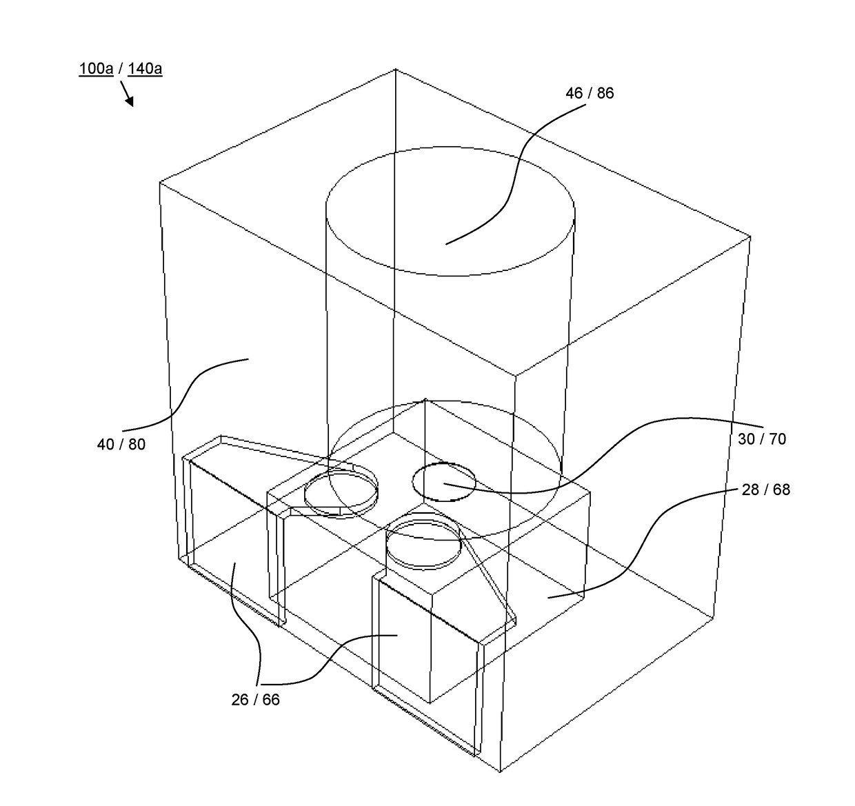
[0093]In order to avoid unnecessary repetitions, the explanations below relate to all seven of the exemplary embodiments of the present invention illustrated on FIG. 5A to FIG. 11C with respect to the configurations, features and advantages of the present invention, unless otherwise indicated:

[0094]The send-site layouts on FIG. 5A to FIG. 11C present respectively a device 100a, 100b, 100c, 100d 100e, 100f, 100g for coupling optical signals into a waveguide 10. The device 100a, 100b, 100c, 100d 100e, 100f, 100g has a send-site circuit (not shown), which based on incoming signals from send-site terminal contacts 22 actuates an electro-optical converter 28, which sends out the optical signals in the direction of the axis 12 of the waveguide 10.

[0095]The receive-site layouts on FIG. 5A to FIG. 11C present respectively a device 140a, 140b, 140c, 140d 140e, 140f, 140g for decoupling optical signals from at least one waveguide 10 in an opto-electrical converter 68, which receives the optic...


PUM


Abstract

In order to further develop a device for coupling optical signals into at least one waveguide, wherein the device comprises at least one electro-optical converter which sends out the optical signals in the direction of the axis or of the core of the waveguide, in such a way that active alignment of the waveguide is not necessary, it is proposedwherein the electro-optical converter is incorporated, in particular embedded, in at least one send-site optical subassembly,wherein the send-site optical subassembly comprises at least one guiding channel for aligning the waveguide with respect to the electro-optical converter, in particular relative to the output port or to the active surface of the electro-optical converter, andwherein at least one extension is assigned to the send-site optical subassembly, in particular to the guiding channel, said extension being provided for aligning the waveguide with respect to the guiding channel.The corresponding is true for a device for decoupling optical signals from at least one waveguide.

Description

CROSS-REFERENCE TO RELATED APPLICATIONS[0001]This application is a continuation of international (WO) patent application no. PCT / DE2015 / 100121, filed 23 Mar. 2015, which claims the priority of German (DE) patent application no. 10 2014 205 373.0, filed 22 Mar. 2014, the contents of each being hereby incorporated herein by reference.FIELD OF THE INVENTION[0002]The present invention basically relates to the technical field of optical sub assemblies (OSA).[0003]More particularly, the present invention relates to a device for coupling optical signals into at least one waveguide, and to a complementary device for decoupling optical signals from at least one waveguide[0004]The present invention further relates to a method for producing such device for coupling / decoupling optical signals into / from at least one waveguide.BACKGROUND OF THE INVENTION[0005]As optical converters, in particular as active optical converters, vertical cavity surface emitting lasers (VCSEL) or photodiodes (PD) send...

Claims


Application Information

Patent Timeline
Patent Type & Authority Applications(United States)
IPC IPC(8): G02B6/42
CPCG02B6/4274G02B6/423
Inventor HOELTKE, HOLGERGROEPL, MARTIN
Owner SILICON LINE
Learn More