Power supply system
- Summary
- Abstract
- Description
- Claims
- Application Information
AI Technical Summary
Benefits of technology
Problems solved by technology
Method used
Image
Examples
first embodiment
Modification of First Embodiment
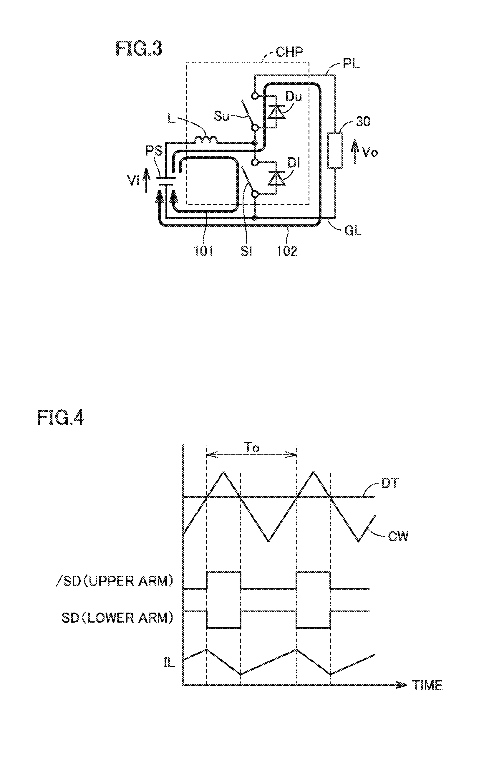
[0230]As described above, in power converter 10 according to the first embodiment, a period during which the second arm is formed is provided, so that a power loss (conduction loss) in the switching element is reduced. On the other hand, as is understood from FIGS. 11, 12, and 15, a period during which the boost chopper circuit having the second arm is formed is limited to a period during which control pulse signals SD1 and SD2 are equal in level to each other.
[0231]Therefore, by securing a period in which control pulse signals SD1 and SD2 are equal in logical level to each other as long as possible under the condition that duty ratios DT1 and DT2 are constant, a power loss in the switching element can further be suppressed.
[0232]In the modification of the first embodiment, a power loss in power converter 10 is further reduced by controlling phases of reactor currents IL1 and IL2 in PWM control for controlling output from DC power supplies B1 and B2.
[...
second embodiment
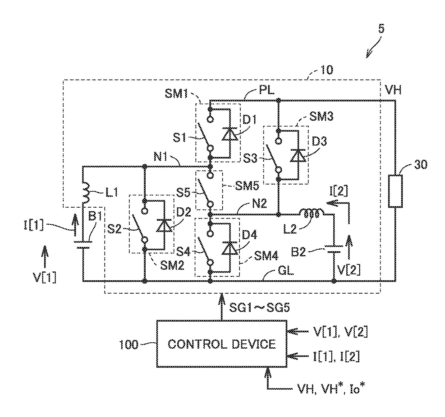
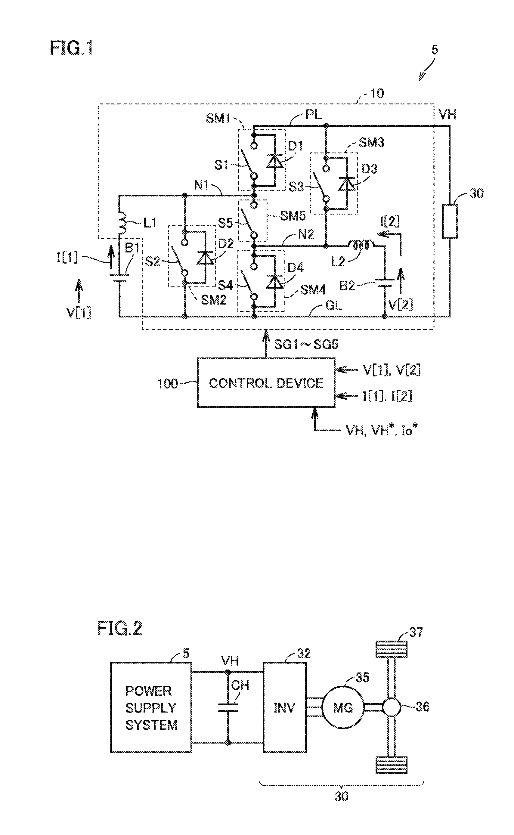
[0263]In a second embodiment, a modification of the circuit configuration of power converter 10 described in the first embodiment will be described. Specifically, a modification in which switching element S5 of power converter 10 shown in FIG. 1 is implemented by a bidirectional switch is shown.
[0264]FIG. 27 is a circuit diagram for illustrating a configuration of a power converter 11 according to the second embodiment.
[0265]Referring to FIG. 27, power converter 11 is different from power converter 10 shown in FIG. 1 in having a bidirectional switch SB5 instead of switching element S5 as a semiconductor element connected between nodes N1 and N2. Namely, bidirectional switch SB5 corresponds to “fifth semiconductor element SM5.” Since other features of power converter 11 are the same as those in power converter 10, detailed description will not be repeated.
[0266]Bidirectional switch SB5 has a diode D5a and a switching element S5a electrically connected in series between nodes N1 and N...
third embodiment
[0280]In a third embodiment, an operation mode other than the parallel boost mode of power converters 10 and 11 described in the first and second embodiments will be described.
[0281]FIG. 29 is a chart showing a list of a plurality of operation modes applied to power converters 10 and 11.
[0282]Referring to FIG. 29, the plurality of operation modes are broadly categorized into a “boost mode” in which output voltage VH is controlled in accordance with voltage command value VH* and a “direct coupling mode” in which on and off of switching elements S1 to S5 (S5a and S5b) is fixed and DC power supply (power supplies) B1 and / or B2 are / is electrically connected to power lines PL and GL.
[0283]The boost mode includes the parallel boost mode described above. In the parallel boost mode, by controlling on and off of switching elements S1 to S5 of power converter 10 in accordance with the gate Boolean expressions shown in FIG. 12, DC / DC conversion can be carried out in parallel between DC power s...
PUM
 Abstract
Description
Claims
Application Information
 - R&D
- Intellectual Property
- Life Sciences
- Materials
- Tech Scout
- Unparalleled Data Quality
- Higher Quality Content
- 60% Fewer Hallucinations
Browse by: Latest US Patents, China's latest patents, Technical Efficacy Thesaurus, Application Domain, Technology Topic, Popular Technical Reports.
© 2025 PatSnap. All rights reserved.Legal|Privacy policy|Modern Slavery Act Transparency Statement|Sitemap|About US| Contact US: help@patsnap.com


