Display device
- Summary
- Abstract
- Description
- Claims
- Application Information
AI Technical Summary
Benefits of technology
Problems solved by technology
Method used
Image

Examples
first embodiment
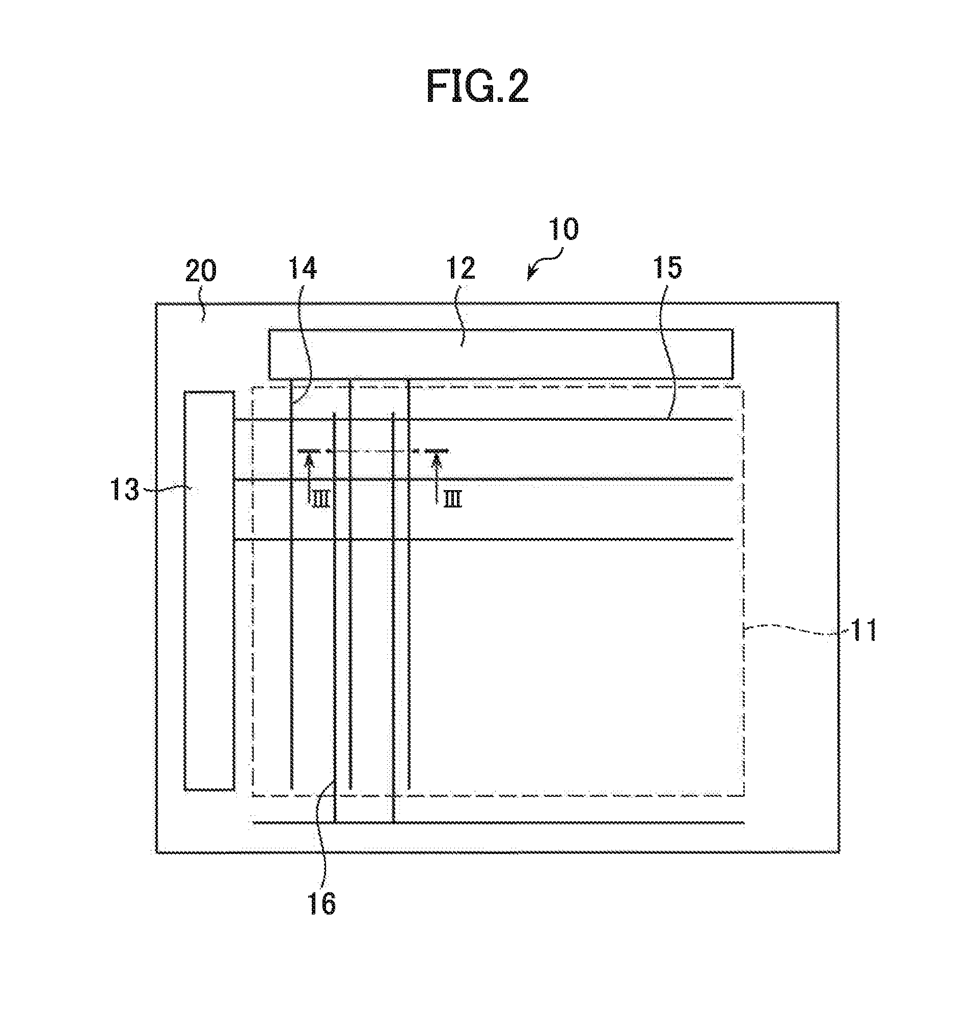
[0033]FIG. 3 is a sectional view of a pixel of the organic EL panel 10 according to a first embodiment of the invention. FIG. 3 is a sectional view which is taken along line III-III in FIG. 2. A substrate 20 is arranged on the lowermost layer of the organic EL panel 10. The substrate 20 is formed using glass, an artificial resin, or the like.
[0034]A base film 21 is formed using SiN, SiO2, or the like, on the substrate 20. A channel layer 32 which electrically connects a drain electrode 30 and a source electrode 33 of the driving transistor is formed on the base film 21. The channel layer 32 is formed using polycrystalline silicon. In addition, the channel layer 32 may be formed using amorphous silicon, or the like. A first insulating film 22 is formed on the base film 21 and the channel layer 32 using SiN, SiO2, or the like. A gate electrode 31 of the driving transistor is formed on the first insulating film 22 using a metal material. A second insulating film 23 is formed on the fir...
second embodiment
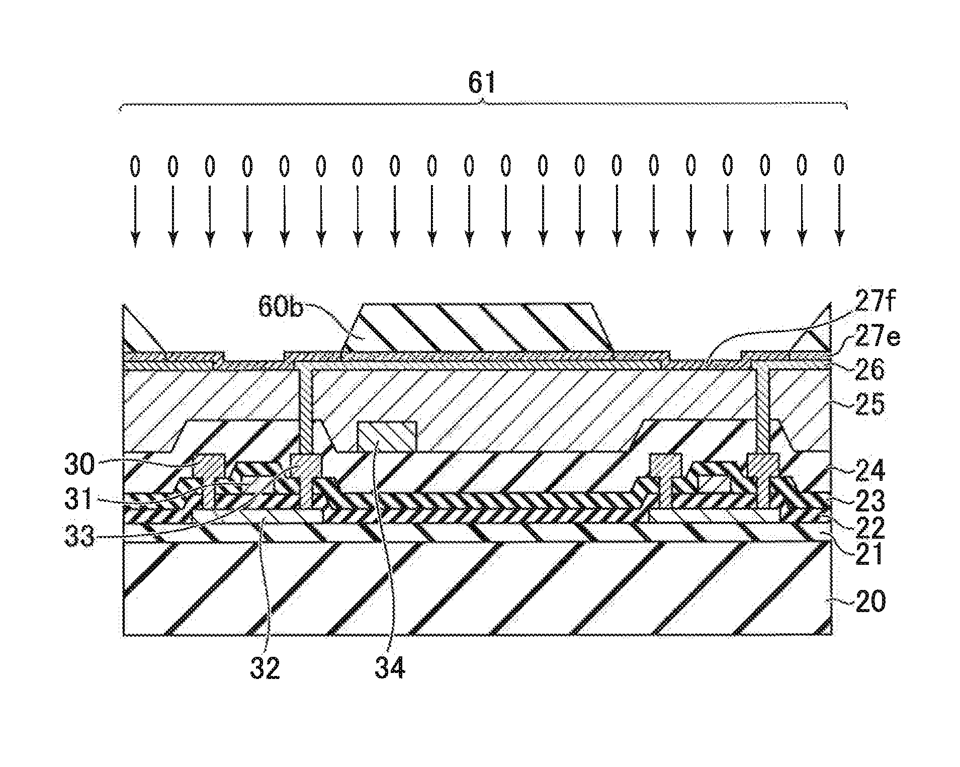
[0048]FIG. 7 is a sectional view of a pixel of an organic EL panel 10 according to a second embodiment. A difference between the organic EL panel 10 according to the second embodiment and the organic EL panel 10 according to the first embodiment is that the hole transport layer 27 is provided over the plurality of pixel electrodes 26, the hole transport layer 27 has an intermediate portion 27f (hereinafter, referred to as intermediate portion 27f) which is provided between adjacent two pixel electrodes 26, and a portion in which carrier mobility is higher than that in the intermediate portion 27f is included at a portion 27e which is provided on the pixel electrode 26 in the hole transport layer 27 (hereinafter, referred to as center portion 27e of hole transport layer). Here, when the hole transport layer 27 is provided over the plurality of pixel electrodes 26, it means that the hole transport layer 27 is continuously provided on the plurality of pixel electrodes 26 in one united ...
third embodiment
[0051]FIG. 8 is a sectional view of a pixel of an organic EL panel 10 according to a third embodiment. In the third embodiment, a configuration in the layers lower than a hole transport layer 27a, a pixel electrode 26, and a planarization film 25 is the same as that in the first embodiment. A plurality of the pixel electrodes 26 are provided by being separated from each other, and the hole transport layers 27a are provided on the respective plurality of pixel electrodes 26 by being separated from each other. For this reason, in the organic EL panel 10 according to the embodiment, a leakage current through the hole transport layer 27a does not occur, and unintended light emitting of a pixel is prevented. The organic EL panel 10 according to the embodiment does not have the pixel separation film 28, and an organic layer 40 is planarly formed on the plurality of hole transport layers 27a and the planarization film 25. According to the embodiment, a light emitting region of the organic ...
PUM
 Abstract
Description
Claims
Application Information
 - R&D
- Intellectual Property
- Life Sciences
- Materials
- Tech Scout
- Unparalleled Data Quality
- Higher Quality Content
- 60% Fewer Hallucinations
Browse by: Latest US Patents, China's latest patents, Technical Efficacy Thesaurus, Application Domain, Technology Topic, Popular Technical Reports.
© 2025 PatSnap. All rights reserved.Legal|Privacy policy|Modern Slavery Act Transparency Statement|Sitemap|About US| Contact US: help@patsnap.com