Liquid crystal display and element substrate thereof

a technology of liquid crystal display and element substrate, which is applied in the direction of electrical equipment, semiconductor devices, instruments, etc., can solve the problems of insufficient capacitance between the bottom conductive layer b>3/b> and the pixel conductive layer b>4/b>, and reduce the reliability of the liquid crystal display, so as to achieve the effect of insufficient capacitan

Active Publication Date: 2016-03-17
INNOLUX CORP
View PDF8 Cites 0 Cited by
  • Summary
  • Abstract
  • Description
  • Claims
  • Application Information

AI Technical Summary

Benefits of technology

This patent is about a method for making a display screen with good transparency and reduced loss of signal. The method involves using a special layer with a specific shape and size, which is placed on top of a metal layer. This layer is made with a process called chemical mechanical planarization. This process removes any uneven surfaces on the metal layer and makes the layer smooth. This layer is important because it helps improve the connection between two other layers, which can help prevent issues like short-circuiting and insufficient capacitance. By using this method, the display screen can have better quality and performance.

Problems solved by technology

However, when the radius of the contact hole 1 at the location of the bottom conductive layer 3 is increased, the capacitance between the bottom conductive layer 3 and the pixel conductive layer 4 is insufficient, and the reliability of the liquid crystal display is decreased.

Method used


Image

  • Liquid crystal display and element substrate thereof
  • Liquid crystal display and element substrate thereof
  • Liquid crystal display and element substrate thereof

Examples


Embodiment Construction

[0017]The following description is of the best-contemplated mode of carrying out the invention. This description is made for the purpose of illustrating the general principles of the invention and should not be taken in a limiting sense. The scope of the invention is best determined by reference to the appended claims.

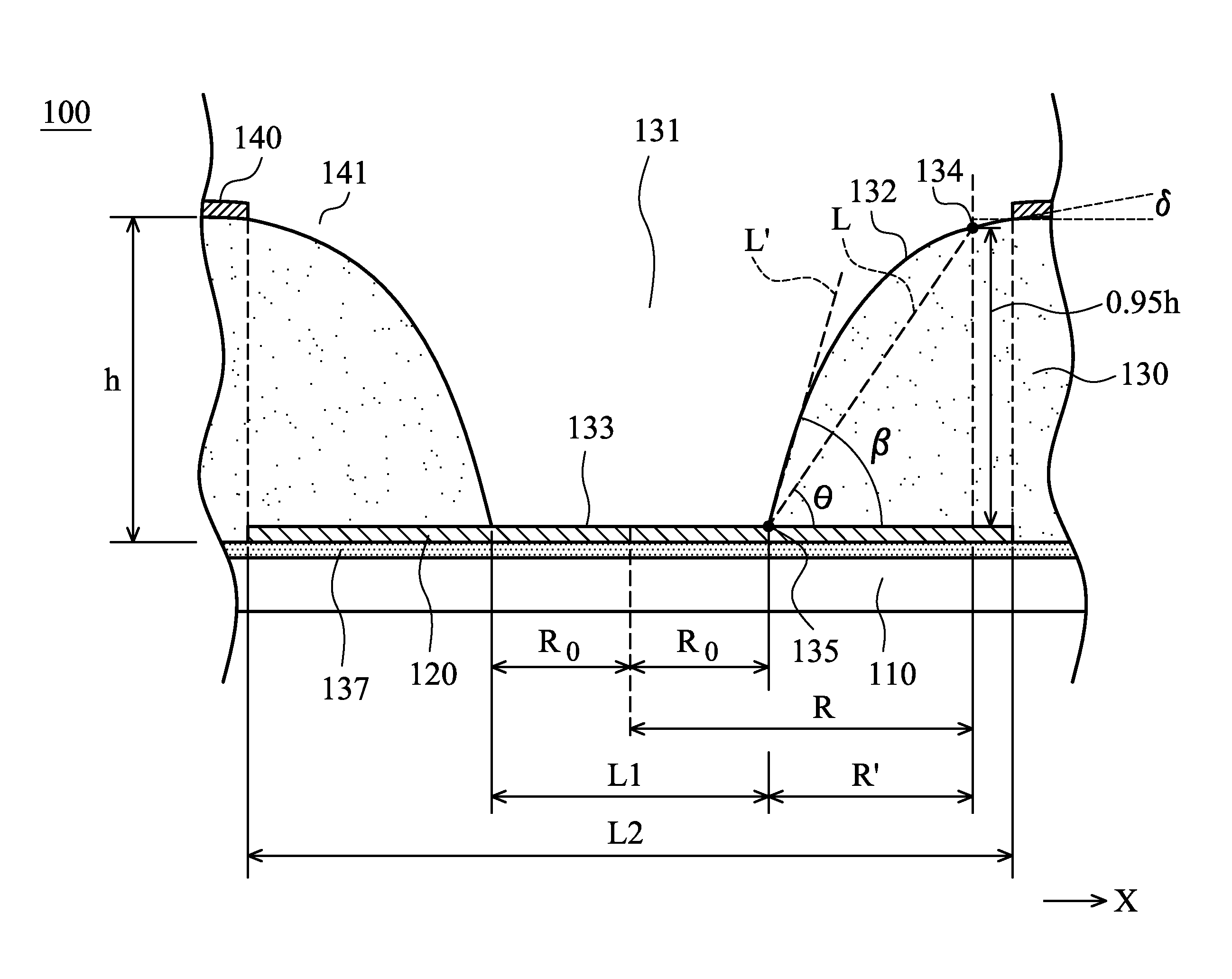
[0018]FIG. 2A shows an element substrate 100 of an embodiment of the invention, which comprises a substrate 110, a metal layer 120, a planarization layer 130 and a first conductive layer 140. The metal layer 120 is disposed on the substrate 110. The planarization layer 130 is located on the metal layer 120, wherein the planarization layer 130 comprises a contact hole 131, the contact hole 131 has a continuous wall 132 and a bottom 133, the bottom 133 exposes the metal layer 120, and the bottom 133 of the contact hole 131 has a first width L1. The first conductive layer 140 is located on the planarization layer 130, wherein the first conductive layer 140 comprises an op...


PUM

PropertyMeasurementUnit
included angleaaaaaaaaaa

Abstract

An element substrate is provided, including a substrate, a metal layer, a planarization layer and a first conductive layer. The metal layer is disposed on the substrate. The planarization layer is located on the metal layer, wherein the planarization layer includes a contact hole, the contact hole has a continuous wall and a bottom, the bottom exposes the metal layer, and the bottom of the contact hole has a first width. The first conductive layer is located on the planarization layer, wherein the first conductive layer includes an opening, the opening exposes the contact hole, and the opening has a second width above the contact hole, wherein the relationship of the first width and the second width is modified to decrease illumination loss and to prevent problems of shot-circuiting and insufficient capacitance.

Description

CROSS REFERENCE TO RELATED APPLICATIONS[0001]This Application claims priority of Taiwan Patent Application No. 103131296, filed on Sep. 11, 2014, the entirety of which is incorporated by reference herein.BACKGROUND OF THE INVENTION[0002]1. Field of the Invention[0003]The present invention relates to a liquid crystal display, and in particular to a liquid crystal display having at least one contact hole.[0004]2. Description of the Related Art[0005]In a liquid crystal display, a contact hole is utilized to conduct a pixel electrode and a source electrode. However, with reference to FIG. 1A, the liquid crystal molecules 2 are arranged along a profile of the contact hole 1, and the contact hole 1 is like a funnel structure.[0006]With reference to FIG. 1B, conventionally, a bottom conductive layer 3 and a pixel conductive layer 4 surround the contact hole. The bottom conductive layer 3 is insulated from the pixel conductive layer 4 by an insulation layer 5. When the radius of the contact...

Claims


Application Information

Patent Timeline
Patent Type & Authority Applications(United States)
IPC IPC(8): H01L27/12G02F1/1368
CPCG02F1/1368H01L27/124G02F1/136227G02F1/134372G02F1/1343G02F1/134363G02F1/13439
Inventor CHUNG, YUEH-TINGHSU, SHAO-WULU, YUNG-HSINCHEN, JYUN-YUCHIU, KUAN-YUWANG, CHAO-HSIANG
Owner INNOLUX CORP
Why Eureka
Try Eureka