
Driving Printed Circuit Board for Display Device and Display Device Having the Same

a technology of printed circuit boards and display devices, which is applied in the direction of printed circuit non-printed electric components, electrical apparatus construction details, instruments, etc., can solve the problems of bringing about various defects in the liquid crystal monitor

Active Publication Date: 2016-03-10
LG DISPLAY CO LTD
View PDF1 Cites 11 Cited by
  • Summary
  • Abstract
  • Description
  • Claims
  • Application Information

AI Technical Summary

Benefits of technology

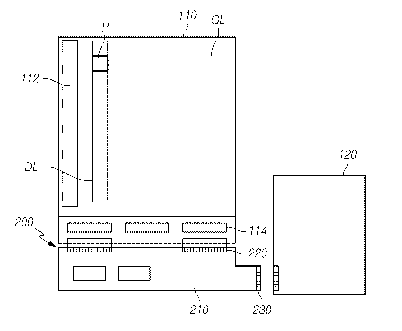
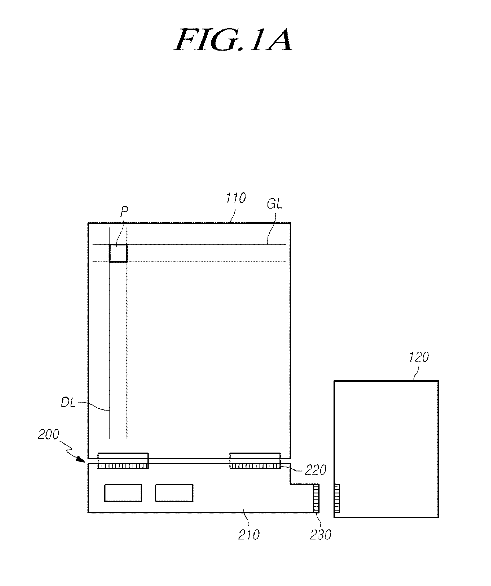
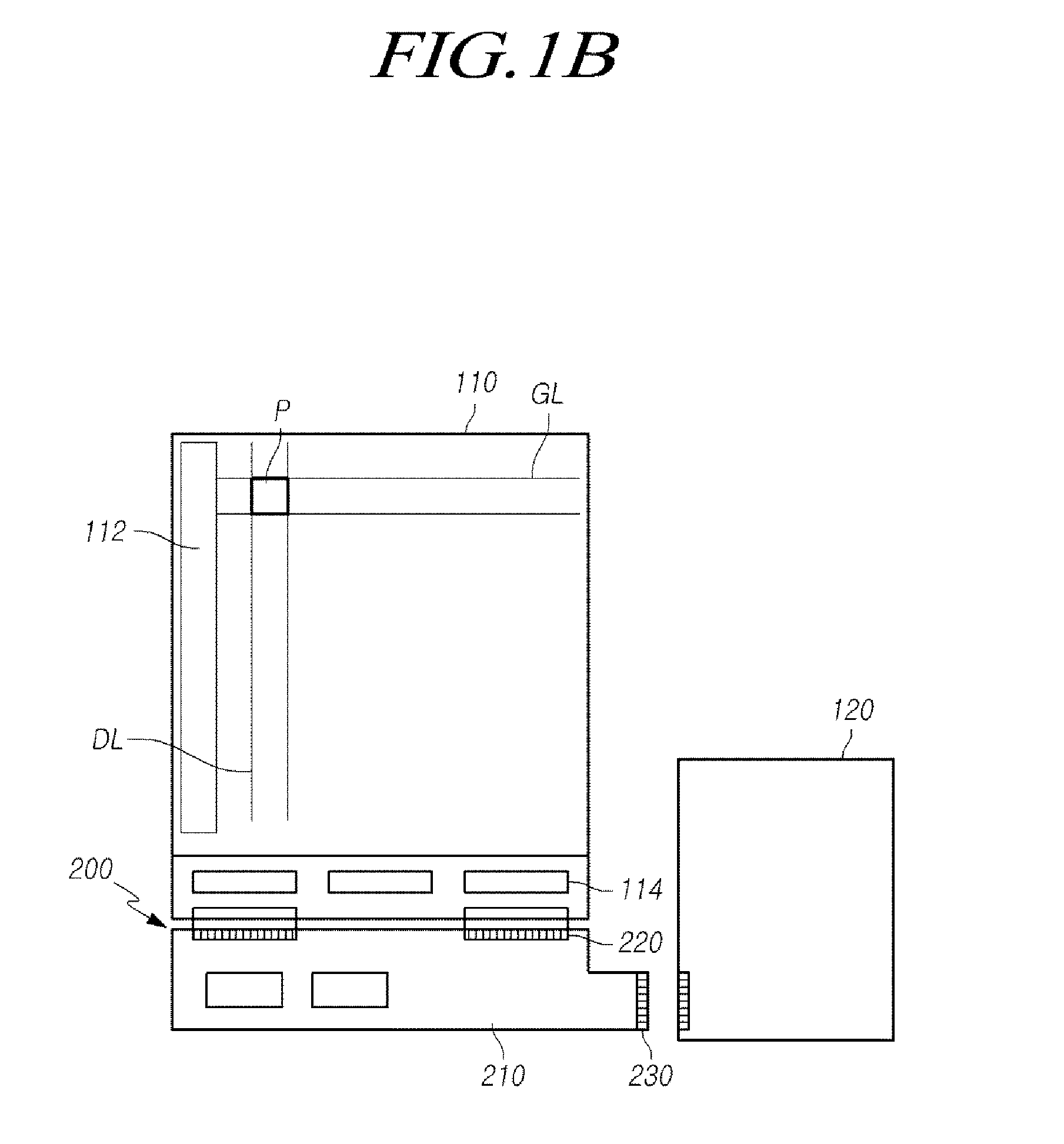
The patent describes an electronic device connection unit and a driving printed circuit board that connect to an electronic device. The connection unit has signal pads and active ground pads that connect to the driving PCB for sending signals. Dummy ground pads without extending onto the driving PCB are also included and connected to the reference voltage of the electronic device through connectors. This design allows for more efficient signaling and better grounding, resulting in improved performance of the electronic device.

Problems solved by technology

Thus, the ground pad may bring about various defects to the liquid crystal monitor.

Method used


Image

  • Driving Printed Circuit Board for Display Device and Display Device Having the Same
  • Driving Printed Circuit Board for Display Device and Display Device Having the Same
  • Driving Printed Circuit Board for Display Device and Display Device Having the Same

Examples


Embodiment Construction

[0024]Hereinafter, embodiments of the present disclosure will be described with reference to the accompanying drawings. In designating elements of the drawings by reference numerals, the same elements will be designated by the same reference numerals although they are shown in different drawings. Further, in the following description of the present disclosure, a detailed description of known functions and configurations incorporated herein will be omitted when it may make the subject matter of the present disclosure rather unclear.

[0025]Furthermore, in the description of the structural elements of the present disclosure, terms of “first”, “second”, “A”, “B”, “(a)”, “(b)” and the like may be used. Each of these terminologies is not used to define an essence, order or sequence of a corresponding component but used merely to distinguish the corresponding component from other component(s). In the case that it is described that a certain structural element “is connected to”, “is coupled ...


PUM


Abstract

An electronic device connection unit includes a substrate and a plurality of signal pads on the substrate configured to send signals from an electronic device to a driving printed circuit board (PCB). One or more active ground pads on the substrate are configured to connect at least the driving PCB to a reference voltage of the electronic device. One or more dummy ground pads on the substrate are configured to connect to the reference voltage of the electronic device without extending onto the driving PCB. One or more connectors are connected to the one or more dummy ground pads, where each of the one or more connectors is configured to electrically couple at least a subset of the one or more dummy ground pads to the one or more active ground pads.

Description

CROSS-REFERENCE TO RELATED APPLICATION[0001]This application claims the benefit under 35 U.S.C. §119(a) of Korean Patent Application No. 10-2014-0119081, filed on Sep. 5, 2014, which is hereby incorporated by reference for all purposes as if fully set forth herein.BACKGROUND OF THE DISCLOSURE[0002]1. Field of the Disclosure[0003]The present disclosure relates to a driving printed circuit board for a display device and a display device having the driving printed circuit board for a display device, and more particularly to a driving printed circuit board (PCB) for connecting an electronic device for a display device to a display panel, and a display device having the driving PCB.[0004]2. Description of the Prior Art[0005]With the development of the information society, various types of requirements for a display device for displaying an image are increasing and, recently, various display devices, such as a liquid crystal display (LCD), a plasma display panel (PDP), and an organic ligh...

Claims


Application Information

Patent Timeline
Patent Type & Authority Applications(United States)
IPC IPC(8): H05K1/02H05K1/11
CPCH05K1/111H05K2201/10128H05K2201/09781H05K1/0296G02F1/13306G02F1/13458H05K2201/09709H05K1/0219H05K1/117H05K1/118H05K2201/09727H05K1/0218H05K1/14H05K2201/04
Inventor YEO, INHOJEON, KYONGSHIK
Owner LG DISPLAY CO LTD
Learn More