
Image processing device and image processing method

Active Publication Date: 2016-03-03
KONICA MINOLTA INC
View PDF1 Cites 0 Cited by
  • Summary
  • Abstract
  • Description
  • Claims
  • Application Information

AI Technical Summary

Benefits of technology

The goal of this invention is to quickly and accurately detect a target image part while using minimal data space.

Problems solved by technology

Image defects such as errors, missing and blots have been detected by reading a printed sheet and checking the obtained image against a checked reference image.
However, determining the feature value of the edge direction requires filtering operations individually for vertical, horizontal and diagonal directions with respective edge detecting filters, which results in the increased number of operations.
Further, since the feature value of the edge intensity has large data volume, a large storage volume is required for storing the feature value, which results in an increased cost.
Furthermore, another problem is that false detection is likely to be increased when a noise is included in the surrounding pixels of a target pixel.
However, the FAST is only a technique for detecting a feature point.

Method used


Image

  • Image processing device and image processing method
  • Image processing device and image processing method
  • Image processing device and image processing method

Examples


Embodiment Construction

[0033]Hereinafter, an embodiment of the image processing device and the image processing method of the present invention will be described referring to the drawings.

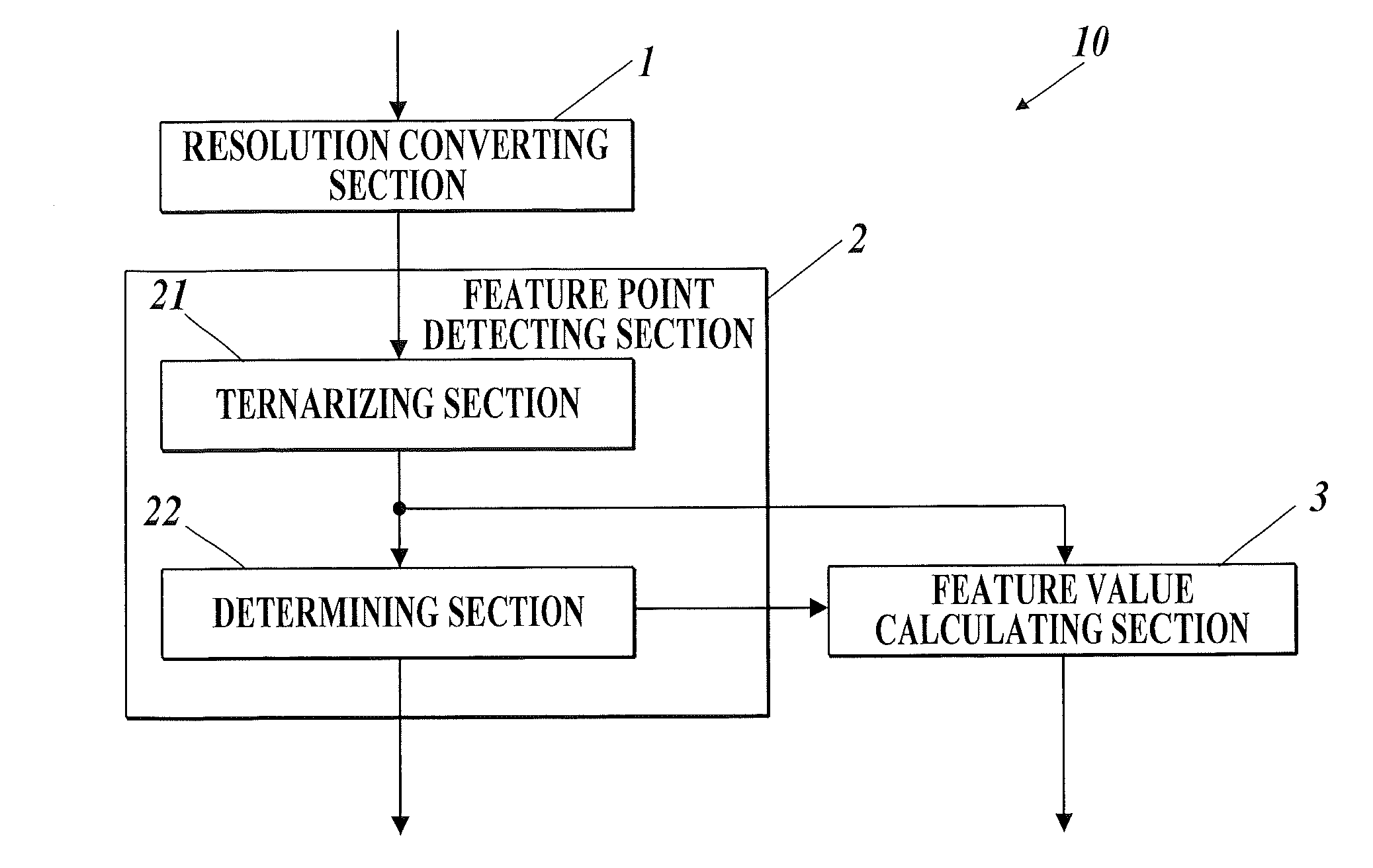
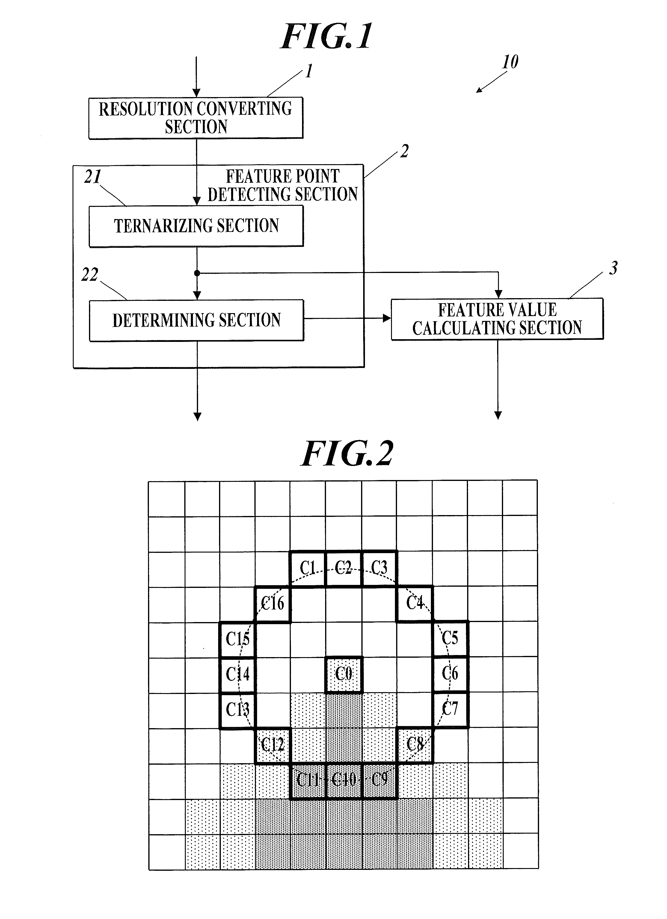
[0034]FIG. 1 is a block diagram of an image processing device 10 according to the present embodiment, illustrating the schematic configuration thereof based on the functionalities.

[0035]The image processing device 10 detects one or more feature point from an image and outputs a calculated feature value of the feature point. As well as characters, figures, photographs and the like of an image, other image parts having a density difference such as blots, stripes and uneven density also have their own image characteristics. Accordingly, it is possible to carry out check, pattern recognition and the like of the image by using their feature values output from the image processing device 10.

[0036]For example, in an image check, the image processing device 10 may detect image defects such as errors, missing and blots by detecti...


PUM


Abstract

An image processing device includes a feature point detecting section which detects a feature point from an image and which includes a ternarizing section and a determining section. The ternarizing section sets each pixel of the image as a target pixel and inputs pixel values of the target pixel and surrounding pixels. The ternarizing section changes each of the pixel values of the surrounding pixels to one of three signal values which represent that brightness of a surrounding pixel is brighter or darker than or similar to brightness of the target pixel. When the number of consecutive surrounding pixels having the same signal value is equal to or greater than a threshold, the determining section determines the target pixel as the feature point.

Description

BACKGROUND OF THE INVENTION[0001]1. Field of the Invention[0002]The present invention relates to an image processing device and an image processing method.[0003]2. Description of Related Art[0004]Image defects such as errors, missing and blots have been detected by reading a printed sheet and checking the obtained image against a checked reference image.[0005]In order to reduce false detection due to a slight displacement of an image, defects have been detected such that a feature point having a unique image characteristic is detected from both images, and the feature value thereof representing the image characteristic is checked.[0006]For example, an edge is detected from an image to be checked as a feature point, and the edge direction and edge intensity of the edge are determined as the feature value (e.g. see JP 2007-156626A).[0007]On the other hand, the FAST (features from accelerated segment test) is known as a method that detects a corner as a feature point (e.g. see Machine ...

Claims


Application Information

Patent Timeline
IPC IPC(8): G06K9/46G06K9/32G06T7/00
CPCG06K9/4638G06K9/4671G06K2009/4666G06T7/003G06K9/4604G06K9/32G06K2009/485G06T2207/20164G06V10/44G06T7/337G06V10/457G06V10/467G06V10/462G06V10/473
Inventor YOSHIZAWA, MASANORI
Owner KONICA MINOLTA INC
Learn More