
Rigid substrate, touch panel, and processing method of rigid substrate

a processing method and substrate technology, applied in the direction of electrical digital data processing, instruments, electrical equipment, etc., can solve the problems of increased possibility of damage to the panel device due to lack of mechanical strength, and different sizes becoming stress concentration areas, etc., to achieve ideal mechanical strength

Active Publication Date: 2015-09-17
TPK HLDG
View PDF10 Cites 0 Cited by
  • Summary
  • Abstract
  • Description
  • Claims
  • Application Information

AI Technical Summary

Benefits of technology

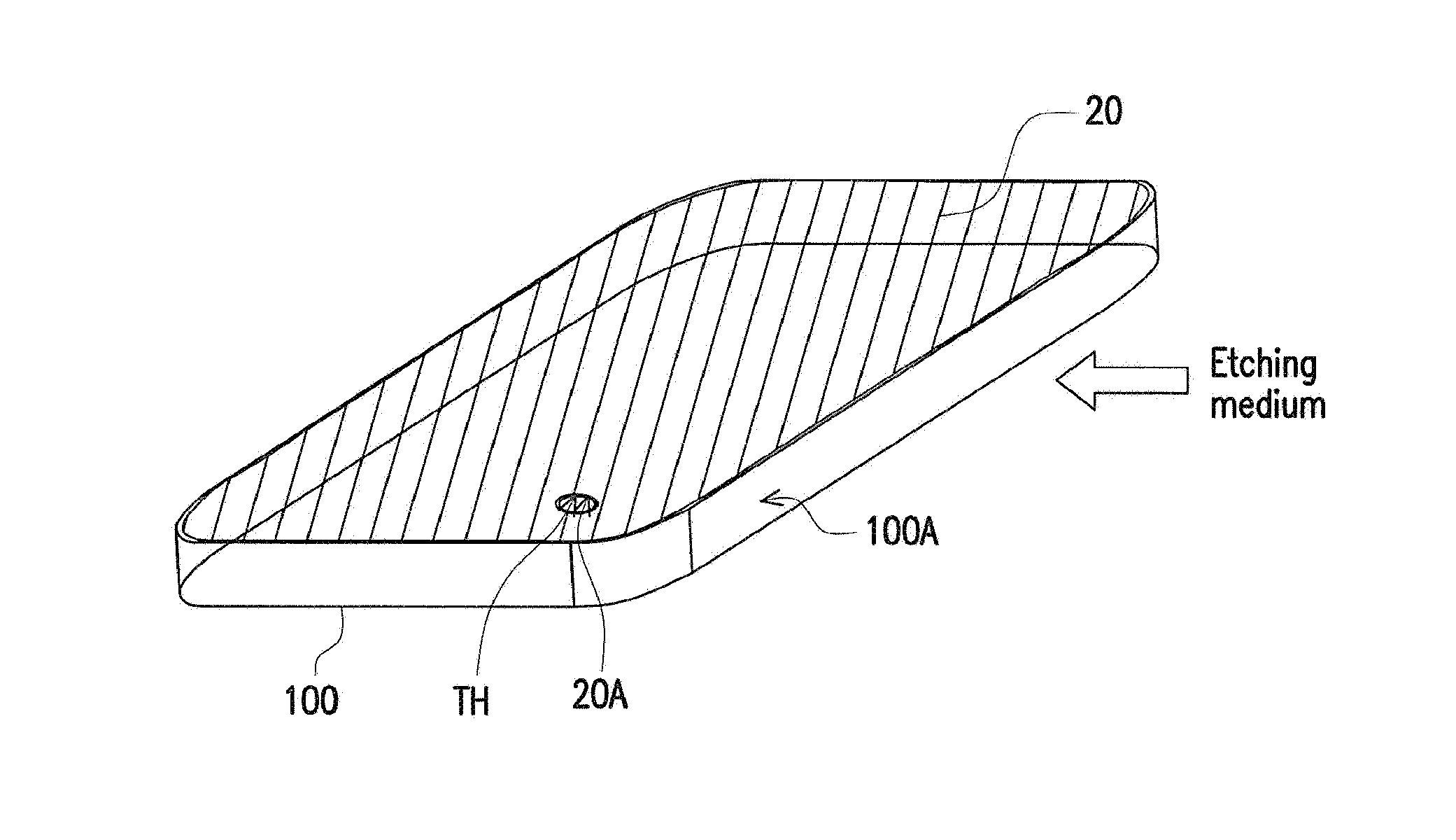
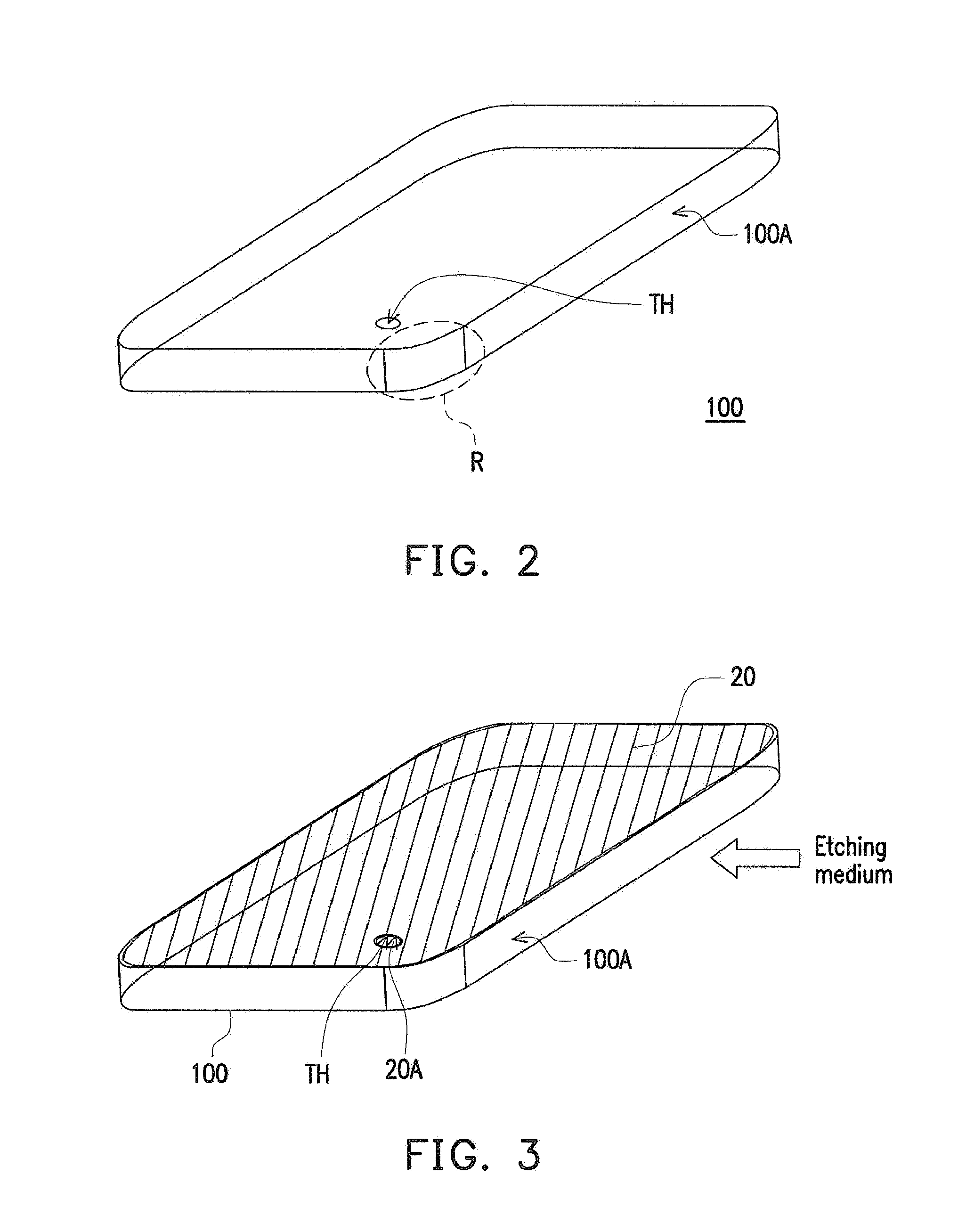
The invention provides a rigid substrate with uniformed cracks that enhance its mechanical strength. This allows for the creation of a high-quality and durable touch panel. The invention also provides a processing method for the rigid substrate that effectively avoids stress concentration phenomena, resulting in an optimal strength. Additionally, the invention offers a method to strengthen the ion strengthened surface layer by performing a chemical strengthening process after the mechanical processed substrate is etched, resulting in a stable product strength.

Problems solved by technology

As probabilities for users to be in direct contact with panel devices significantly increase, possibilities of damaging the panel devices due to lack of mechanical strength may also increase.
Nevertheless, the strengthened substrate generally has to undergo a process of cutting and forming so as to comply with a designed size of a product, a plurality of cracks with different sizes are produced at cut-off edges during the process of cutting and forming, and the cracks with different sizes often become stress concentration areas.
Therefore, the aforementioned substrate still has some limits as in enhancing the mechanical strength of the panel devices; and especially, the substrate often starts to crack from the cut-off edges.

Method used


Image

  • Rigid substrate, touch panel, and processing method of rigid substrate
  • Rigid substrate, touch panel, and processing method of rigid substrate
  • Rigid substrate, touch panel, and processing method of rigid substrate

Examples


Embodiment Construction

[0033]It is noted that a depth of an ion strengthened surface layer of a glass in embodiment of the invention is referring to an average depth of potassium ions diffusing from the outer surface into the interior of the glass, and a better definition is referring to an average value of maximum diffusion depths of the potassium ion when a plurality of areas are divided out on the entire outer surface of the glass. The depth of the ion strengthened surface layer generally may be obtained by utilizing an instrument to detect whether the potassium ions are present. Since even under a same manufacturing process the diffusion depths of the ions would still vary, the invention adopts the average value of the diffusion depths as a standard for determining the depth of the ion strengthened surface layer.

[0034]Namely, in an embodiment, the depth of the ion strengthened surface layer may be defined as a value obtained from averaging the corresponding measured depths of a plurality of measuring ...


PUM

PropertyMeasurementUnit
surface roughnessaaaaaaaaaa
aperture sizesaaaaaaaaaa

Abstract

A rigid substrate, a touch panel including the rigid substrate and a processing method of the rigid substrate are provided. The rigid substrate includes an ion strengthened surface layer completely covering the entire outer surface thereof. The rigid substrate has an etched wall, wherein an average depth of the ion strengthened surface layer on the etched wall is substantially equivalent to an average depth of the ion strengthened surface layer outside of the etched wall.

Description

CROSS-REFERENCE TO RALATED APPLICATIONS[0001]This application is a divisional of Prior application Ser. No. 13 / 950,139, filed on May 30, 2013, which claims the benefit of Taiwan application serial no. 101119366, filed on May 30, 2012 by the present inventor, the disclosure of which are incorporated herein by referenceBACKGROUND OF THE INVENTION[0002]1. Field of the Invention[0003]The invention relates to a substrate, a touch panel, and a processing method of the substrate. More particularly, the invention relates to a rigid substrate, a touch panel including the rigid substrate, and a processing method of the rigid substrate.[0004]2. Description of the Related Art[0005]As probabilities for users to be in direct contact with panel devices significantly increase, possibilities of damaging the panel devices due to lack of mechanical strength may also increase. Therefore, the mechanical strength of the panel devices has become an important factor in indicating a durability of electronic...

Claims


Application Information

Patent Timeline
Patent Type & Authority Applications(United States)
IPC IPC(8): C03C21/00G09G5/00G06F3/047C03C15/00C03C19/00
CPCC03C21/002C03C15/00C03C19/00G06F2203/04103G09G5/003G09G2300/0426G06F3/047C03C15/02C03C2204/08G06F3/0443G06F3/0445Y10T428/239H01H9/02H01H11/00
Inventor LEE, CHIA-HUANGWU, MING-KUNGKUO, HENG-CHIA
Owner TPK HLDG
Learn More