


Quick Research
Generate reliable direction feasibility study reports for your R&D in just a few steps.

Technical Q&A
Discover and master advanced knowledge NOW. Basics, ideas, possibilities, all at once.

Find Solutions
As an expert in R&D theories, this can generate solutions to your technical problems instantly.

Evaluate Feasibility
Analyze your overall solution with one click, know your potential R&D risks in advance.

Monitor Landscape
Get weekly tech updates, stay abreast of the latest tech innovations and key insights.
Copper Tube Interconnect
a copper tube and interconnect technology, applied in the field of semiconductor devices, can solve the problems of limited bandwidth of such stacked die modules, power and bandwidth constraints imposed by power requirements, minimum device footprint requirements, physical limitations of conductor-based connections,
- Summary
- Abstract
- Description
- Claims
- Application Information
AI Technical Summary
Benefits of technology
Problems solved by technology
Method used
Image

Examples
Embodiment Construction
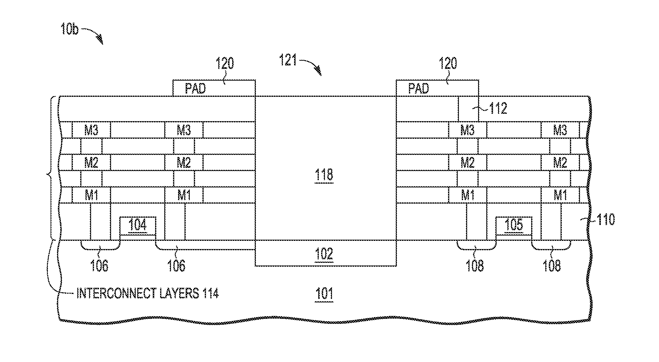
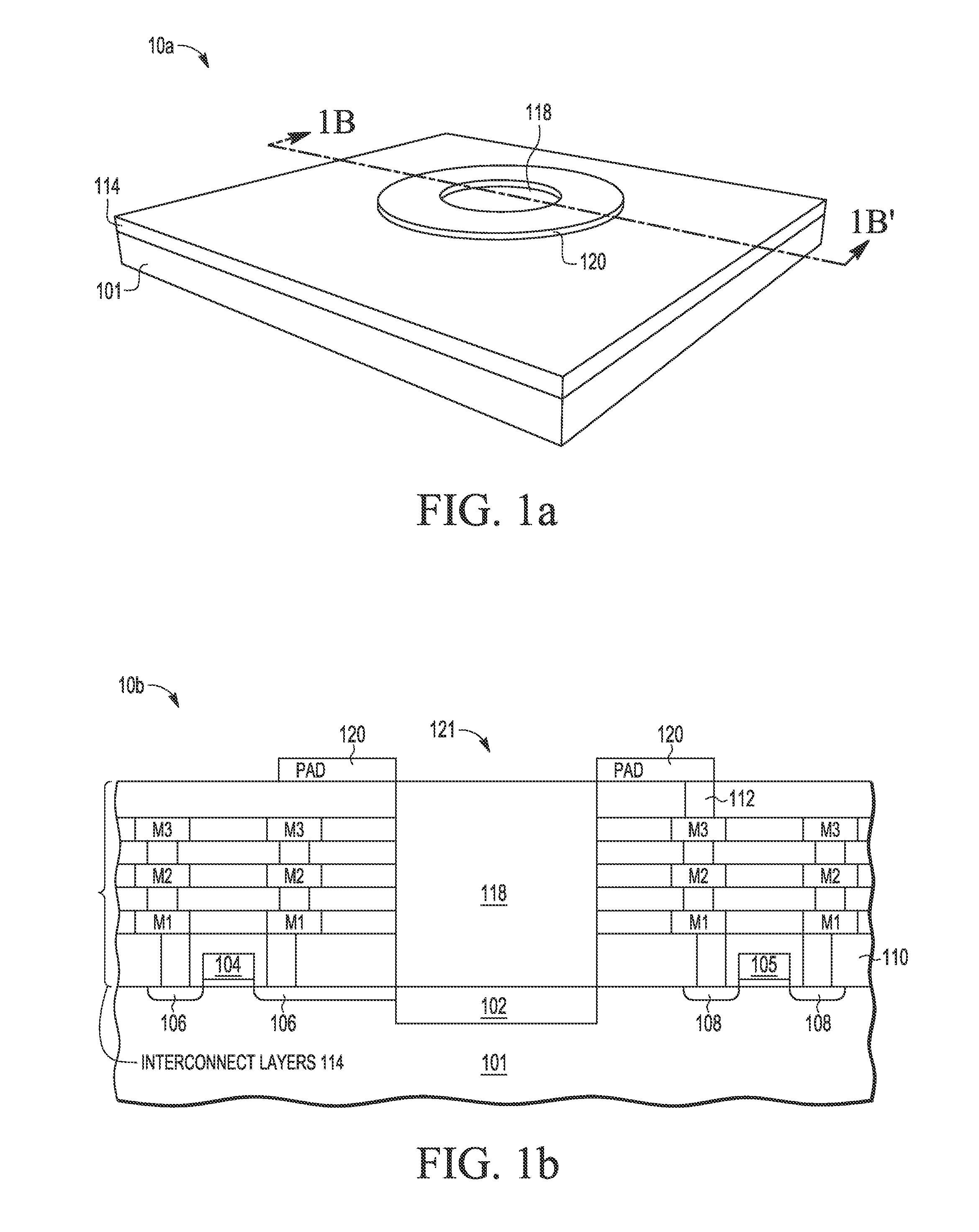
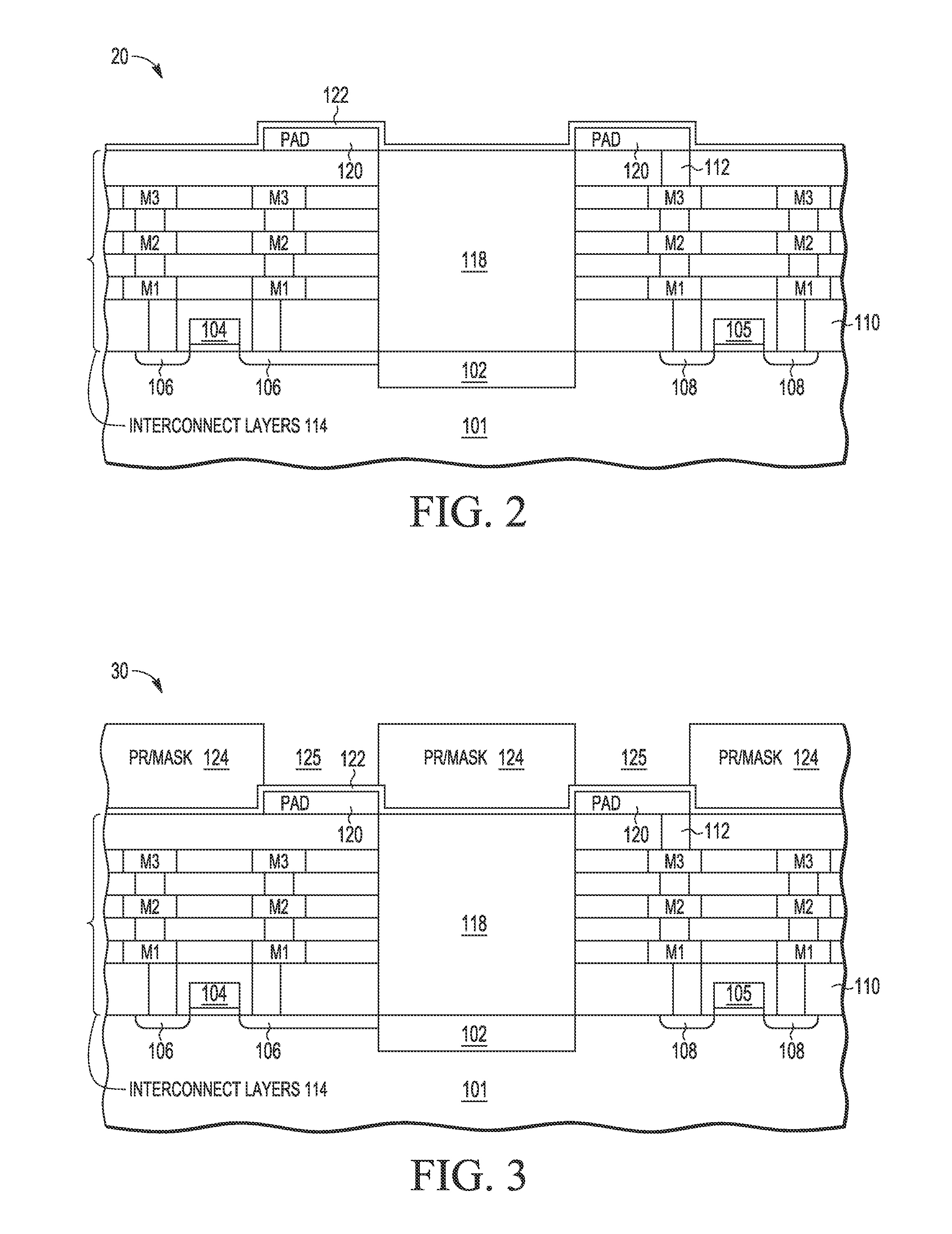
[0016]A method and apparatus are described for fabricating conductive tube interconnect structures that may be at least partially filled with an optical conducting medium or air gap for use in transferring data and / or power between multiple die or between a die and package substrate using electrical and optical signals conveyed through the conductive tube interconnect structures. In selected embodiments, each conductive tube interconnect structure is formed by electroplating or otherwise depositing copper, aluminum, or other suitable electrically conductive materials to fill at least part of a tube mold structure formed over an optical component in the integrated circuit die or wafer, thereby forming an electrically conductive cylindrical interconnect structure. In addition, at least part of each conductive tube interconnect structure may be filled with an optically transparent medium, such as glass, optically clear epoxies, air, or any suitable optical material, thereby forming an ...
PUM
 Abstract
Description
Claims
Application Information
 - R&D Engineer
- R&D Manager
- IP Professional
- Industry Leading Data Capabilities
- Powerful AI technology
- Patent DNA Extraction
Browse by: Latest US Patents, China's latest patents, Technical Efficacy Thesaurus, Application Domain, Technology Topic, Popular Technical Reports.
© 2024 PatSnap. All rights reserved.Legal|Privacy policy|Modern Slavery Act Transparency Statement|Sitemap|About US| Contact US: help@patsnap.com