
Vcsel with intracavity contacts

a vcsel and intracavity technology, applied in semiconductor lasers, laser details, electrical apparatus, etc., can solve the problems of low power conversion efficiency, low production cost of vcsel arrays, difficult competition with high-power laser bars, etc., to achieve easy serial connection, safe environment, and high voltage

Active Publication Date: 2015-05-21
TRUMPF PHOTONIC COMPONENTS GMBH
View PDF3 Cites 3 Cited by
  • Summary
  • Abstract
  • Description
  • Claims
  • Application Information

AI Technical Summary

Benefits of technology

The present invention provides a new design for VCSELs that have intracavity contacts, which improves efficiency and reduces absorption losses. This design allows for a thinner mirror with a high reflectivity, which saves material and production costs. The use of oxide layers in the mirrors allows for a higher voltage application and enables serial connection of multiple VCSELs. The metallic contacts on the sides of the VCSELs facilitate electrical connection between them. The use of a metallization structure on one side of the VCSEL array provides mechanical stability without the need for a supporting substrate. The proposed design also reduces the complexity of the epitaxial design and allows for the growth of well-suited materials.

Problems solved by technology

Commercially available state of the art VCSELs suffer from too low power conversion efficiency so that competition with high power laser bars is difficult.
Although the production costs for VCSEL arrays are relatively low, the fraction cost per output power is in tight competition with conventional light sources.

Method used


Image

  • Vcsel with intracavity contacts
  • Vcsel with intracavity contacts
  • Vcsel with intracavity contacts

Examples


Embodiment Construction

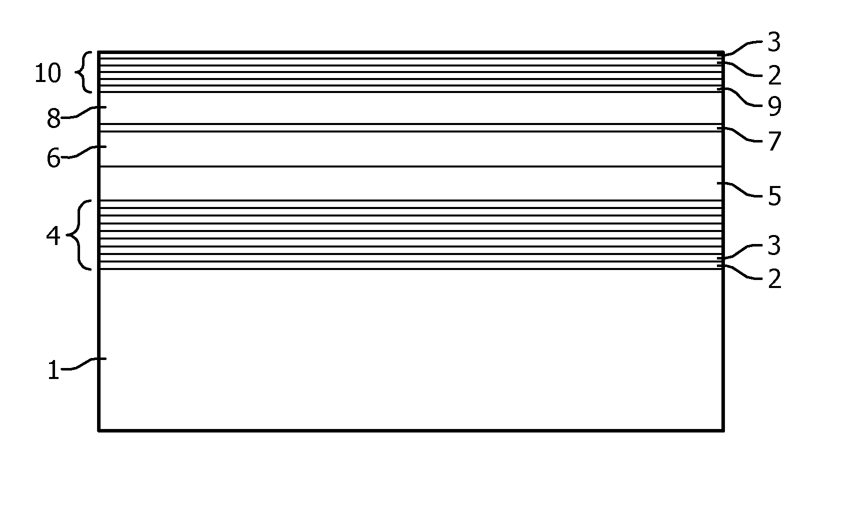
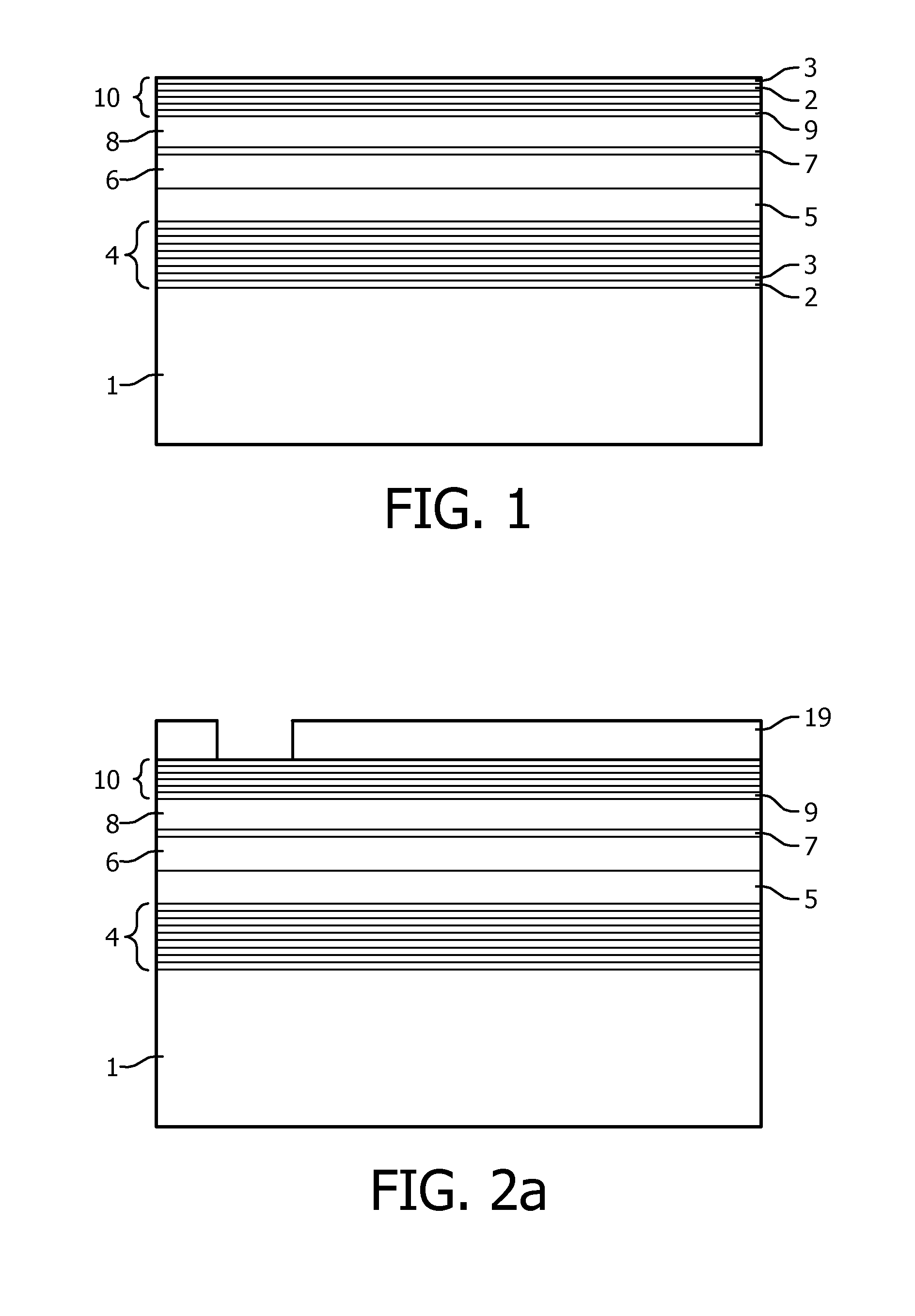
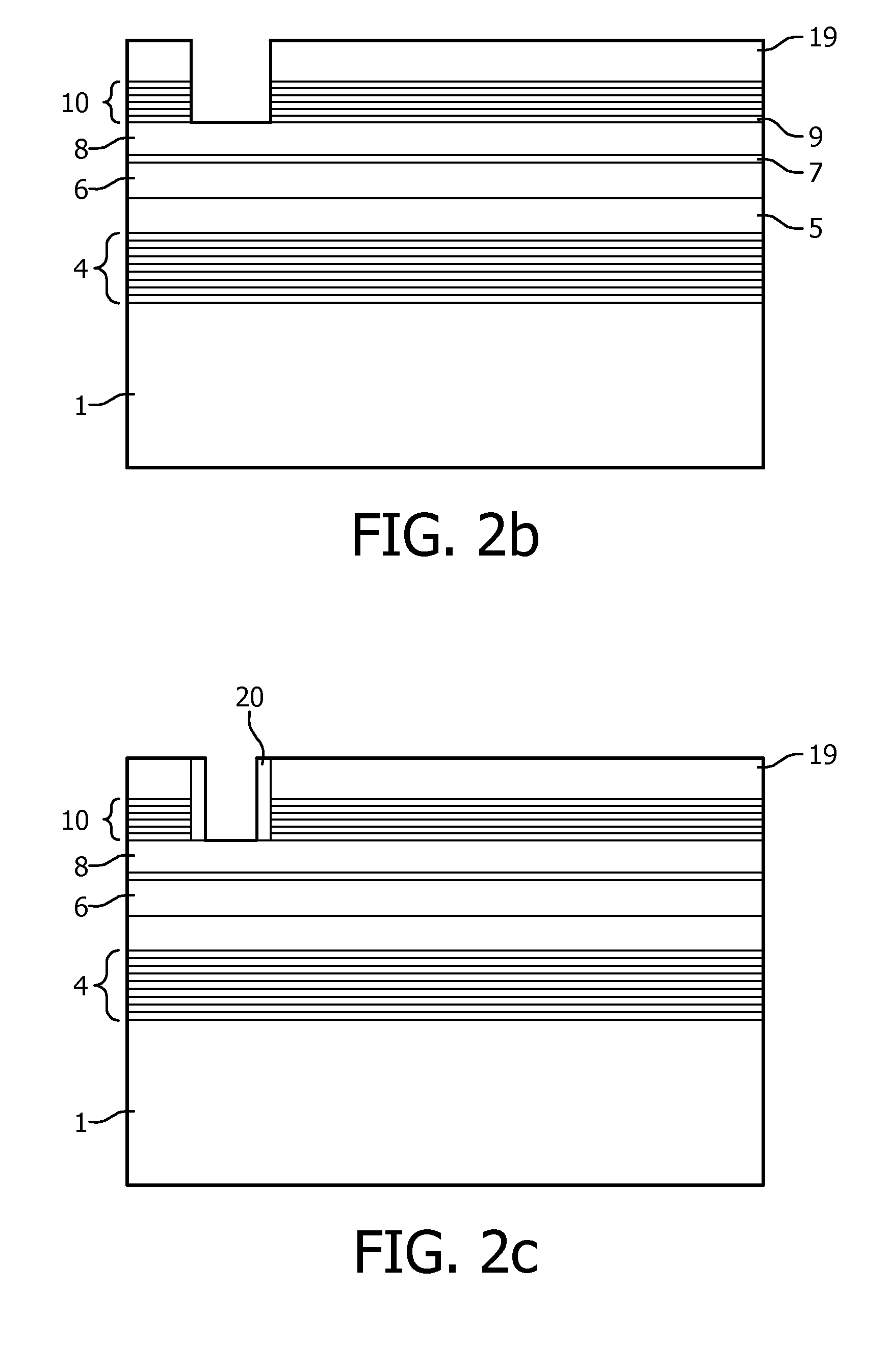
[0019]FIG. 1 schematically shows an example of an epitaxial layer structure for forming a proposed VCSEL as a top emitter. The epitaxial layer design starts with pairs of AlAs / Al(x)Ga(1−x)As layers (0≦x≦0.3) on a GaAs substrate 1. The combination of AlAs-layers 2 with the Al(x)Ga(1−x)As layers, for example GaAs-layers 3, gives a high contrast DBR with high reflectivity after converting the AlAs-layers 2 from AlAs to Aluminum oxide. For short wavelength VCSELs, the GaAs-layers should be exchanged by some AlGaAs-layers to avoid fundamental absorption in the mirrors. In order to achieve a high reflectivity, eight pairs of AlAs / GaAs-layers are used in this example.

[0020]On top of this bottom DBR 4 a Si-doped spacer region is arranged forming the n-current-injection layer 5. The doping profile periodically varies in the direction of the optical axis of the VCSEL which is perpendicular to the layers and substrate 1. The variation is such that higher doping concentrations are situated in m...


PUM


Abstract

The present invention relates to a laser device being formed of at least one VCSEL (15) with intracavity contacts. The VCSEL comprises a layer structure (18) with an active region (6) between a first DBR (4) and a second DBR (10), a first current-injection layer (5) of a first conductivity type between the first DBR (4) and the active region (6), and a second current-injection layer (8) of a second conductivity type between the second DBR (10) and the active region (6). The first and second current-injection layers (5, 8) are in contact with a first and a second metallic contact (11, 12), respectively. The first and / or second DBR (4, 10) are formed of alternating Aluminum oxide and Al(x)Ga(1−x)As containing layers. The proposed design of this VCSEL allows an increased efficiency and lower production costs of such a laser since the top and bottom DBRs may be formed of a considerable reduced thickness.

Description

FIELD OF THE INVENTION[0001]The present invention relates to a laser device being formed of at least one vertical cavity surface emitting laser (VCSEL) with intracavity contacts, said VCSEL comprising a layer structure with an active region between a first distributed Bragg reflector (DBR) and a second distributed Bragg reflector, a first current-injection layer of a first conductivity type between the first distributed Bragg reflector and the active region, and a second current-injection layer of a second conductivity type between the second distributed Bragg reflector and the active region, said first and second current-injection layers being in contact with a first and a second metallic contact, respectively.BACKGROUND OF THE INVENTION[0002]Commercially available state of the art VCSELs suffer from too low power conversion efficiency so that competition with high power laser bars is difficult. Although the production costs for VCSEL arrays are relatively low, the fraction cost pe...

Claims


Application Information

Patent Timeline
Patent Type & Authority Applications(United States)
IPC IPC(8): H01S5/187
CPCH01S5/187H01S5/0217H01S5/18311H01S5/18341H01S5/18347H01S5/18358H01S5/18372H01S5/305H01S5/4018H01S5/423H01S5/04257H01S5/0234H01S5/183
Inventor GERLACH, PHILIPP HENNINGWEIGL, ALEXANDERWIMMER, CHRISTIAN
Owner TRUMPF PHOTONIC COMPONENTS GMBH
Learn More