Titanium incorporation into absorber layer for solar cell
a solar cell and absorber layer technology, applied in the field of photovoltaic devices and fabrication methods, can solve the problems of large vsub>oc/sub>deficit of czts devices, difficult to achieve an efficiency above 11%, and low performance of czts solar cells
- Summary
- Abstract
- Description
- Claims
- Application Information
AI Technical Summary
Problems solved by technology
Method used
Image
Examples
example 1
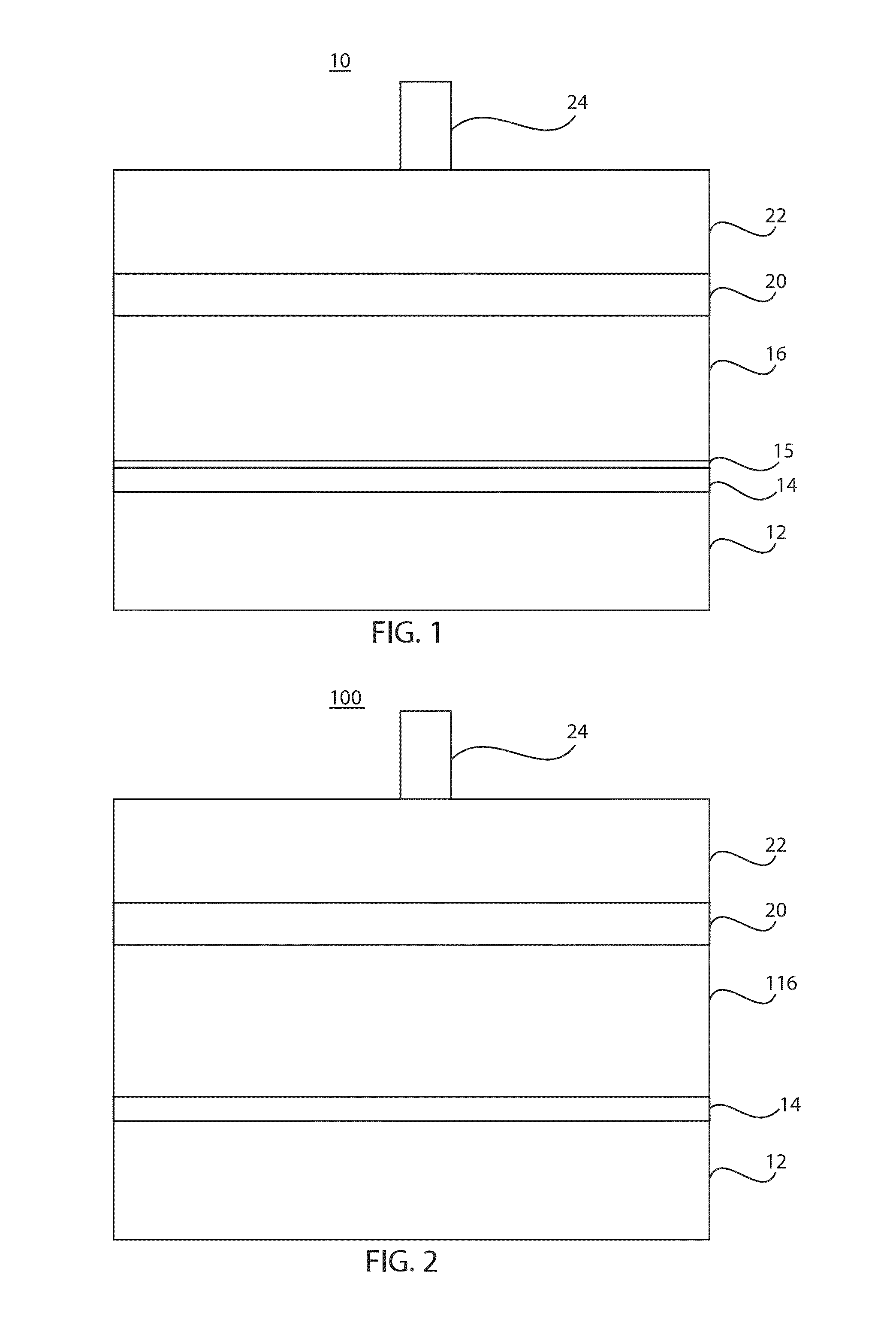
[0056]For making Ti-free devices, solution A (3.3M Cu2S) was made by dissolving Cu and S in hydrazine. Similarly, Sn and Se were stirred in hydrazine to form slurry B (1.5 M SnSe8); Solution A and slurry B were mixed together and transferred to a vial containing zinc formate, yielding solution C with final composition Cu / (Zn+Sn)=0.8, Zn / Sn=1.22 and nominal kesterite CZTSSe concentration of approximately 0.4 M. The thin film CZTS absorber layer with final thickness of 2-2.5 microns was prepared by spin coating this mixture over six consecutive layers at 600 rpm and then subsequently subjecting it to a short anneal on a ceramic hot plate with a set point of 630 degrees C.
[0057]The CdS buffer, ZnO window, and indium doped tin oxide (ITO) layers were subsequently deposited by chemical bath deposition and RF magnetron sputtering, respectively, giving a CZTSSe device structure with a device area of approximately 0.45 cm2, as defined by mechanical scribing. A Ni / Al collection grid and 110-...
example 2
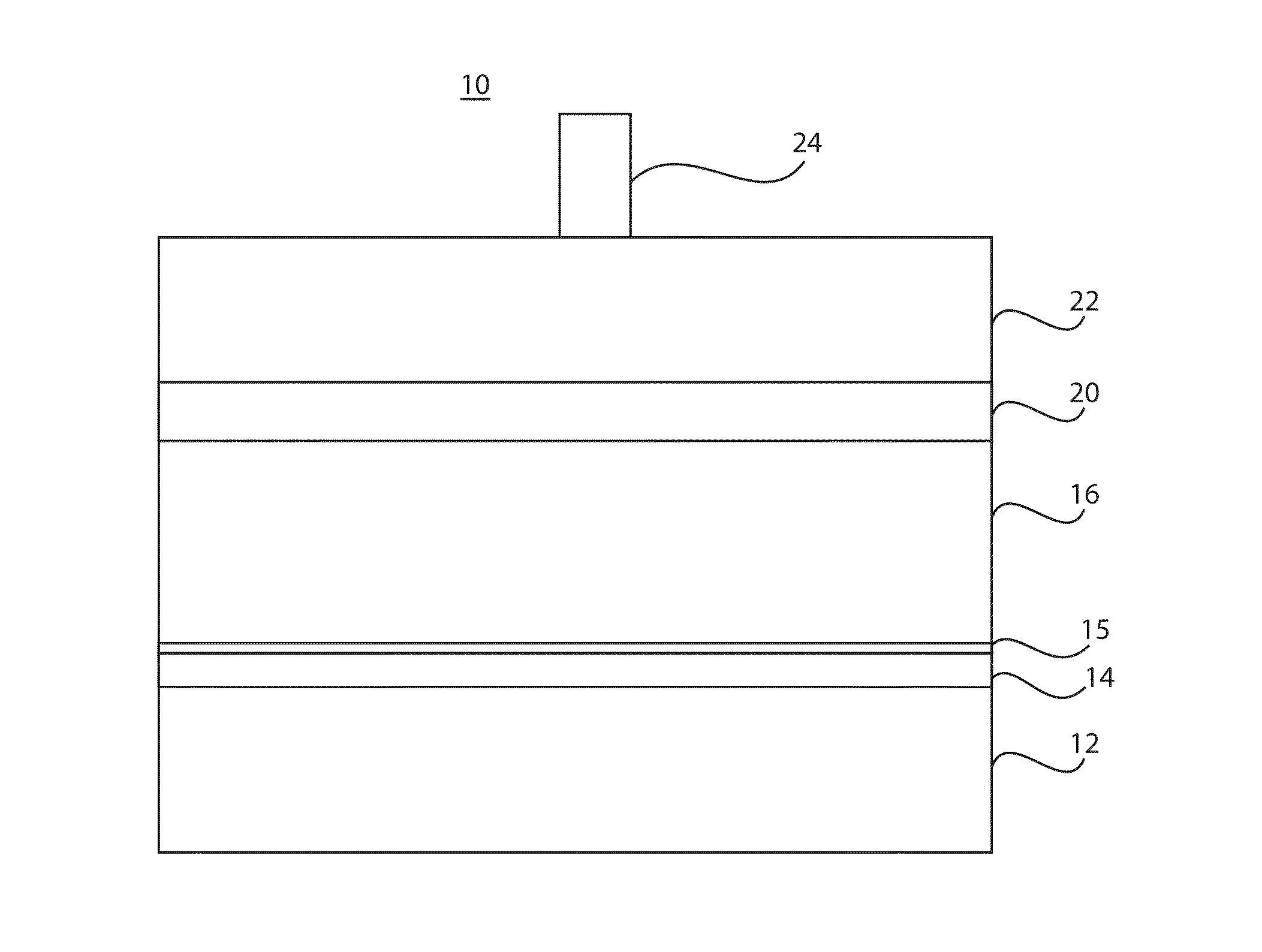
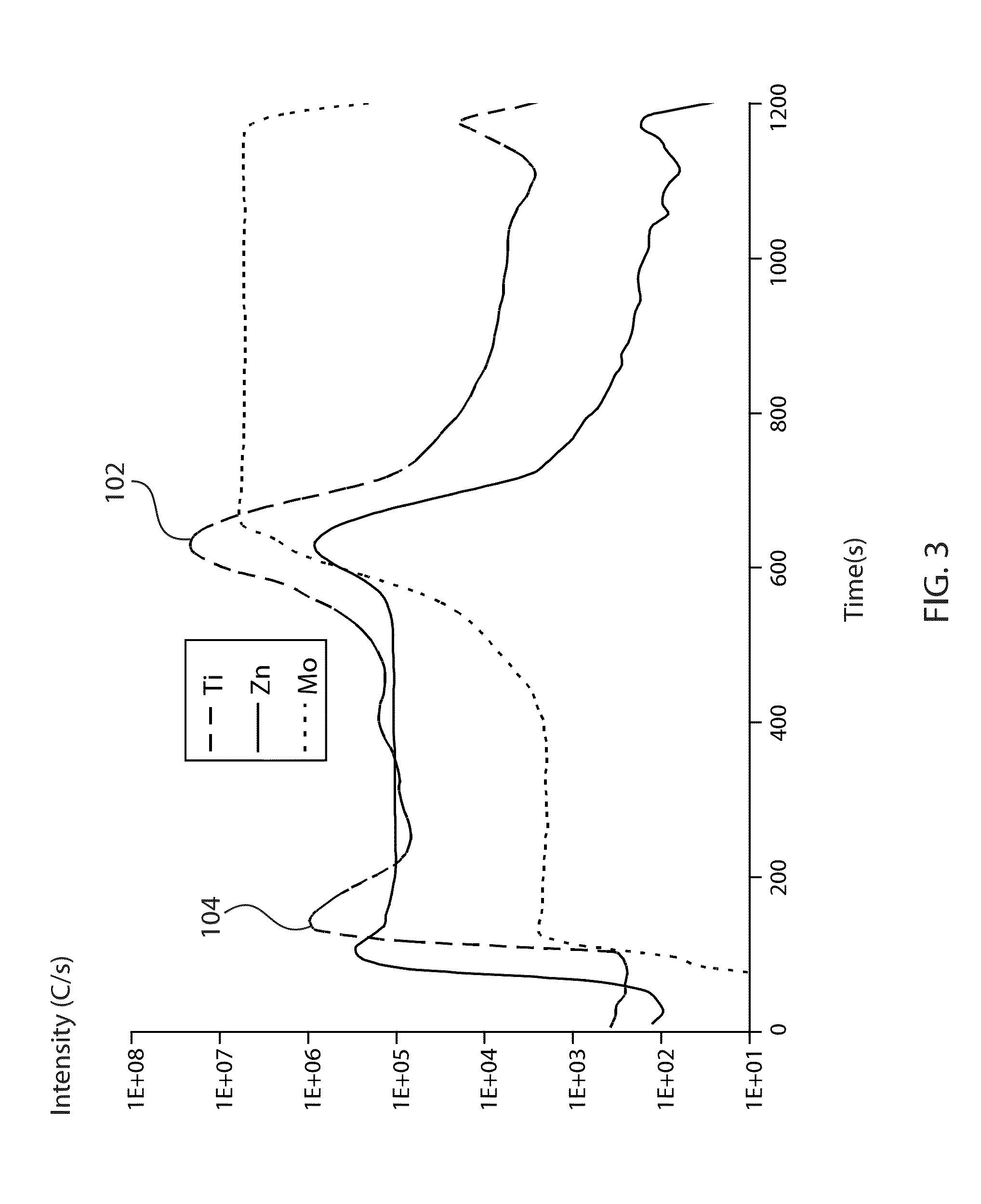
[0058]For making Ti-incorporating devices, a solution A (3.3M Cu2S) was made by dissolving Cu and S in hydrazine. Similarly, Sn and Se were stirred in hydrazine to form slurry B (1.5 M SnSe8); Solution A and slurry B were mixed together and transferred to a vial containing zinc formate, yielding solution C with final composition Cu / (Zn+Sn)=0.8, Zn / Sn=1.22 and nominal kesterite CZTSSe concentration of approximately 0.4 M. A 20 nm titanium thin film was deposited on molybdenum-coated glass by electron-beam evaporation. The Ti- and Mo-coated glass was used as a substrate for CZTS deposition.
[0059]The thin film CZTS absorber layer with final thickness of 2-2.5 microns was prepared by spin coating this mixture over six consecutive layers at 600 rpm and then subsequently subjecting it to a short anneal on a ceramic hot plate with a set point of 630 degrees C. The CdS buffer, ZnO window, and indium doped tin oxide (ITO) layers were subsequently deposited by chemical bath deposition and RF ...
PUM
 Abstract
Description
Claims
Application Information
 - R&D
- Intellectual Property
- Life Sciences
- Materials
- Tech Scout
- Unparalleled Data Quality
- Higher Quality Content
- 60% Fewer Hallucinations
Browse by: Latest US Patents, China's latest patents, Technical Efficacy Thesaurus, Application Domain, Technology Topic, Popular Technical Reports.
© 2025 PatSnap. All rights reserved.Legal|Privacy policy|Modern Slavery Act Transparency Statement|Sitemap|About US| Contact US: help@patsnap.com


