Contact prevention film, touch panel and display device cover panel
a technology of contact prevention film and touch panel, which is applied in the direction of instruments, coatings, and details of portable computers, etc., can solve the problems of black stains, small optical protrusions of antireflection film, and easy crushing of antireflection film, etc., to achieve small haze value, prevent black stains, and improve optical properties of coherence prevention film.
- Summary
- Abstract
- Description
- Claims
- Application Information
AI Technical Summary
Benefits of technology
Problems solved by technology
Method used
Image
Examples
first embodiment
[0098](First Embodiment of the Display Device)
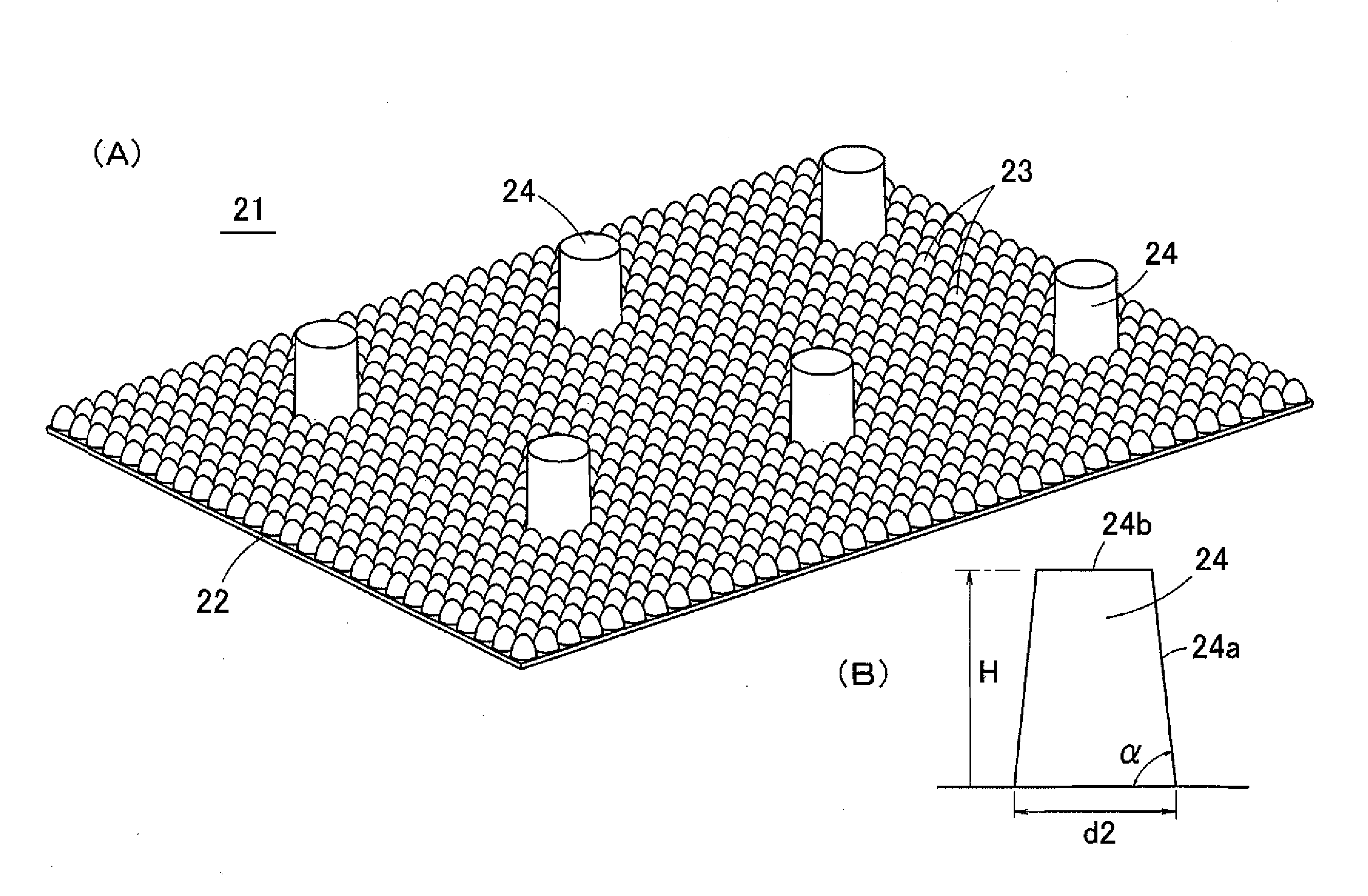
[0099]FIG. 14(A) and FIG. 14(B) show a first embodiment of the display device affixed with the antireflection film 21 according to the present invention. The display device 31 as shown in FIG. 14(A) is obtained by overlapping a cover panel 33 to a front surface of an image display panel 32 such as a liquid crystal display panel (LCD) or organic EL (OLED) with an air gap (space) interposed between, and the antireflection film 21 is affixed onto a rear surface of the cover panel 33. The display device 31 as shown in FIG. 14(B) is affixed with the antireflection film 21 on the front surface of the image display panel 32. In this respect, the image display panel 32 might be either for monochrome display or for color display. The cover panel 33 is a protection sheet of uniform thickness made of transparent resin.
[0100]In the antireflection film 21 of the present invention, the difference in optical properties such as reflectance and haze valu...
second embodiment
[0105](Second Embodiment of the Display Device)
[0106]FIG. 17(A) shows a second embodiment of the display device affixed with the antireflection film 21 according to the present invention. This display device 41 is obtained by overlapping a touch panel 42 to a front surface of an image display panel 32 such as a liquid crystal display panel (LCD) or organic EL (OLED) with an air gap (space) interposed between, and the antireflection film 21 is affixed onto a rear surface of the touch panel 42.
[0107]As shown in FIG. 17(A), the touch panel 42 comprises a touch panel substrate 43 that propagates surface acoustic waves and a sheet material 44 that is disposed to oppose the touch panel substrate 43 and that can contact the touch panel substrate 43 by pressing. A peripheral edge portion of the touch panel substrate 43 and a rear surface peripheral edge portion of the sheet material 44 are joined by a spacer 50 of frame-like shape, and a closed space surrounded by the spacer is formed betwe...
PUM
| Property | Measurement | Unit |
|---|---|---|
| Fraction | aaaaa | aaaaa |
| Fraction | aaaaa | aaaaa |
| Angle | aaaaa | aaaaa |
Abstract
Description
Claims
Application Information
 - R&D
- Intellectual Property
- Life Sciences
- Materials
- Tech Scout
- Unparalleled Data Quality
- Higher Quality Content
- 60% Fewer Hallucinations
Browse by: Latest US Patents, China's latest patents, Technical Efficacy Thesaurus, Application Domain, Technology Topic, Popular Technical Reports.
© 2025 PatSnap. All rights reserved.Legal|Privacy policy|Modern Slavery Act Transparency Statement|Sitemap|About US| Contact US: help@patsnap.com


