Color filtering array substrate and the manufacturing method thereof

Active Publication Date: 2015-01-15
SHENZHEN CHINA STAR OPTOELECTRONICS TECH CO LTD
View PDF1 Cites 3 Cited by
  • Summary
  • Abstract
  • Description
  • Claims
  • Application Information

AI Technical Summary

Benefits of technology

The invention provides a color filtering array substrate and a manufacturing method that reduces the electrical field intensity and improves the display performance of the substrate. By arranging a color filtering layer between a first metallic layer and a second metallic layer, the distance between the first and second peripheral metallic layers in the non-display area is increased, which decreases the electrical field intensity and reduces the ESD effect and signal influence between the layers. The manufacturing method is simple and efficient, and the display performance and lifetime of the substrate are also improved. This reduces the cost of manufacturing the substrate.

Problems solved by technology

Such ESD effect may cause the liquid crystal panel malfunction.
However, the voltage difference (U) between the gate metallic layer 100 and the source / drain metallic layer 200 is unpredictable and uncontrollable.
However, the above configuration may result in electrostatic effect in the interleaved portions between the gate metallic layer and the source / drain metallic layer, and which will shorten the lifetime of the liquid crystal panel.

Method used


Image

  • Color filtering array substrate and the manufacturing method thereof
  • Color filtering array substrate and the manufacturing method thereof
  • Color filtering array substrate and the manufacturing method thereof

Examples


Embodiment Construction

[0069]Embodiments of the invention will now be described more fully hereinafter with reference to the accompanying drawings, in which embodiments of the invention are shown.

[0070]In one embodiment, the ESD effect is reduced by increasing the distance between two ends (the first peripheral metallic layer 21 and the second peripheral metallic layer 26).

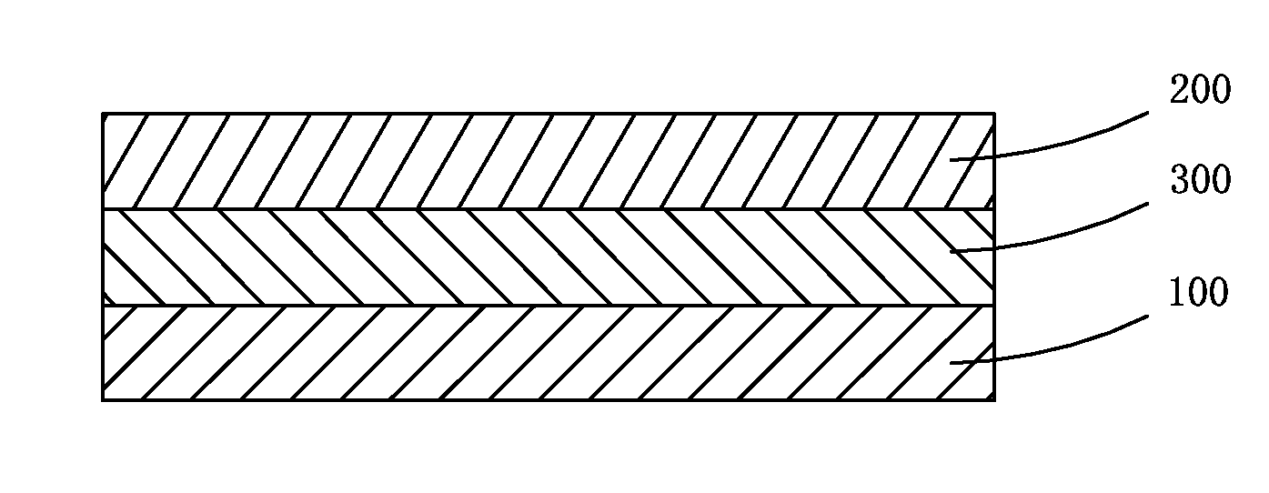
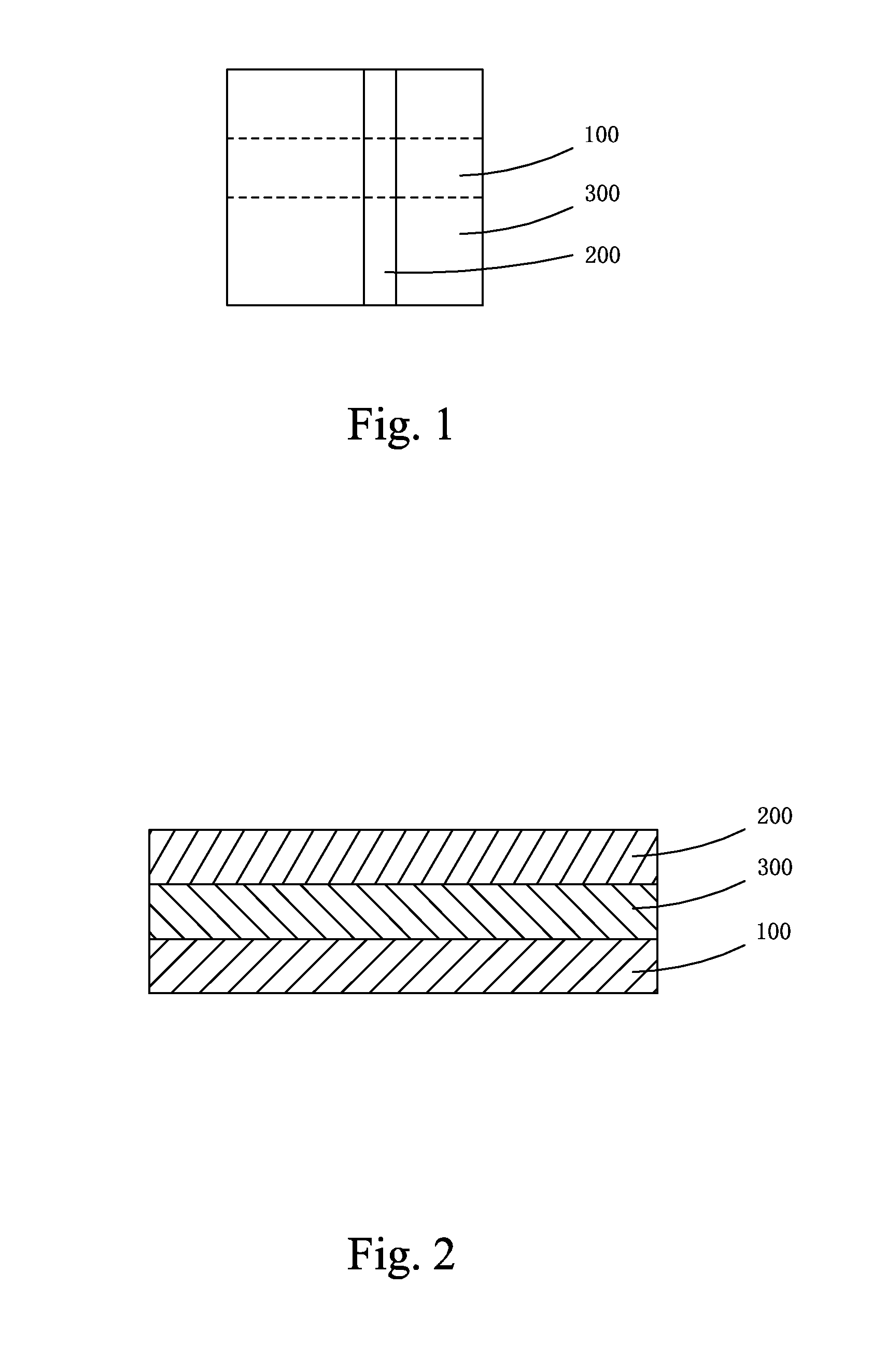
[0071]FIGS. 4 to 6 show the color filtering array substrate in accordance with one embodiment. Though the color filtering array substrate relates to the COA technology, but the color filtering array substrate is different from the conventional color filtering array substrate. By arranging the color filtering layer 23 between the first metallic layer and the second metallic layer, the blocking portion 50 of the color filtering layer 23 is arranged in the interleaved portions of the first peripheral metallic layer 21 and the second peripheral metallic layer 26 in the non-display area. In this way, the distance between the first peripheral...


PUM


Abstract

A color filtering array substrate and the manufacturing method thereof are disclosed. The color filtering array substrate includes a glass substrate (20) having a display area and a non-display area, a first metallic layer above the glass substrate, an insulation layer (22) above the first metallic layer, a second metallic layer above the insulation layer (22), a color filtering layer (23) formed between the insulation layer (22) and the second metallic layer, and a transparent conductive layer above the second metallic layer. The first metallic layer is for forming a first peripheral metallic layer (21) in the non-display area and to form a first internal metallic layer in the display area. The second metallic layer is for forming a second peripheral metallic layer (26) in the non-display area and to form a second internal metallic layer in the display area. The color filtering layer includes a color portion arranged in the display area and a blocking portion arranged in an interleaved portion of the first peripheral metallic layer and the second peripheral metallic layer.

Description

BACKGROUND OF THE INVENTION[0001]1. Field of the Invention[0002]The present disclosure relates to liquid crystal display technology, and more particularly to a color filtering array substrate and the manufacturing method thereof.[0003]2. Discussion of the Related Art[0004]Liquid crystal displays (LCDs) typically are characterized by attributes including thin, power-saving, and low radiation. Thus, the LCDs are widely adopted by a plurality of electronic devices, such as mobile phones, PDA, digital cameras, displays of personal computers or notebooks.[0005]Currently, most of the LCDs are backlight-type LCDs. Generally, the LCDs include a housing, a liquid crystal panel and a backlight module arranged within the housing. The liquid crystal panel includes a color filtering array substrate, a Thin Film Transistor (TFT) Array Substrate, and a liquid crystal layer arranged therebetween. By applying driving voltages toward the two substrates to control the alignment of the liquid crystal, ...

Claims


Application Information

Patent Timeline
IPC IPC(8): G02F1/1335G02B5/20
CPCG02F1/133516G02B5/201G02F1/133514G02F1/133512G02F1/133388
Inventor DONG, CHENGCAI
Owner SHENZHEN CHINA STAR OPTOELECTRONICS TECH CO LTD
Why Eureka
Try Eureka