Photovoltaic mobile device
a mobile device and photovoltaic technology, applied in the field of mobile devices, can solve problems such as greater power consumption, and achieve the effect of reducing the charging frequency of the mobile device and prolonging the standby tim
- Summary
- Abstract
- Description
- Claims
- Application Information
AI Technical Summary
Benefits of technology
Problems solved by technology
Method used
Image
Examples
first embodiment
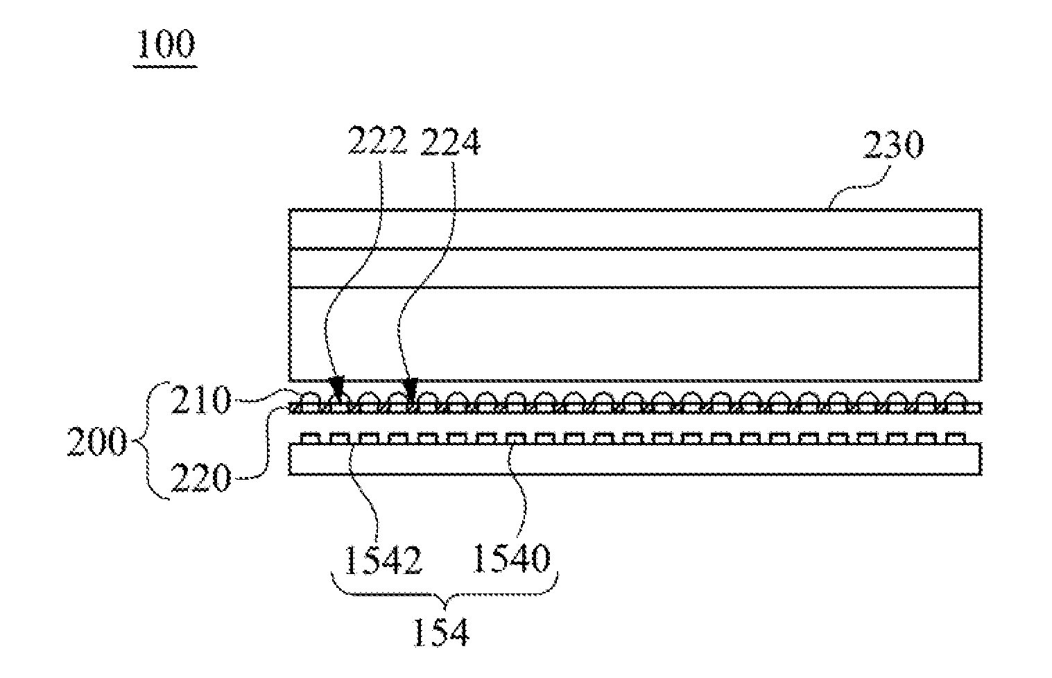
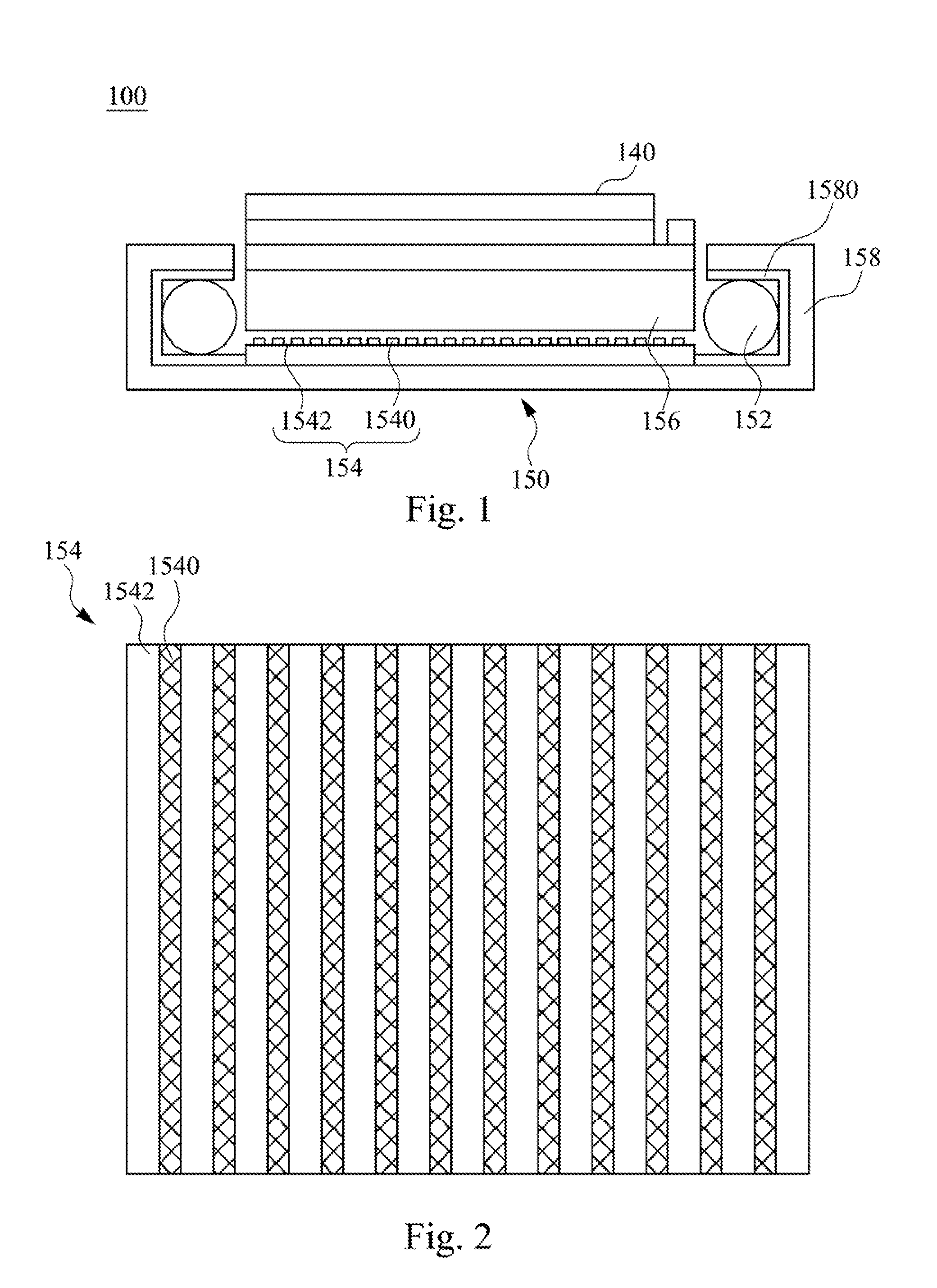
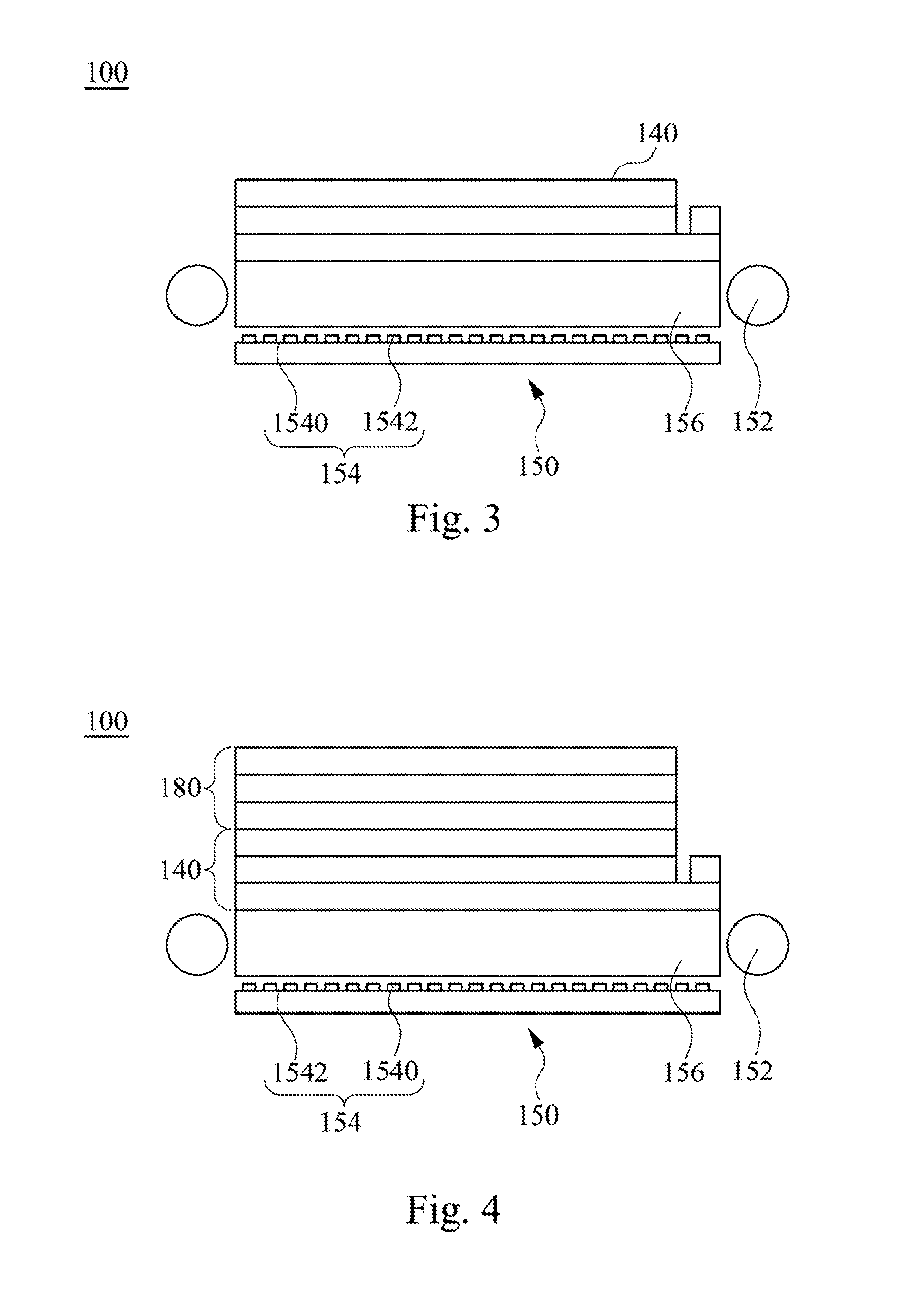
[0031]FIG. 1 is a cross-sectional schematic view of a photovoltaic mobile device of the invention. The photovoltaic mobile device 100 includes a backlight module 150 and a liquid crystal display panel 140. The liquid crystal display panel 140 is disposed above the backlight module 150. The backlight module 150 includes a plurality of light sources 152, a photovoltaic substrate 154 including a plurality of strip type photovoltaic components 1540 and a plurality of reflection strips 1542, and a light guide plate 156. The light sources 152 are disposed at opposite sides of the light guide plate 156. The light sources 152 are disposed in a light source bracket 158 The photovoltaic substrate 154 is disposed between the light source bracket 158 and the light guide plate 156. The photovoltaic mobile device further includes a photovoltaic layer 1580. The photovoltaic layer 1580 is coated on an inner surface of the light source bracket 158 facing the light sources 152.
[0032]The backlight mod...
fourth embodiment
[0038]FIG. 5 is a cross-sectional schematic view of the photovoltaic mobile device 100 of the invention. In addition to the touch panel 180, the photovoltaic mobile device 100 may further include a 3D-barrier 190. The 3D-barrier 190 is disposed above the backlight module 150. In this embodiment, the 3D-barrier 190 is disposed between the liquid crystal panel 140 and the touch panel 180.
[0039]The 3D-barrier 190 may include a plurality of optical gratings. The 3D-barrier 190 is utilized to change the optical path of the light emitted from the liquid crystal display panel 140, thereby providing a 3D image for viewing by a user.
[0040]The 3D barrier 190, the liquid crystal display panel 140, and the touch panel 180 can be three separate elements. Alternatively, the 3D-barrier 190 can be integrated with the liquid crystal display panel 140. For example, a bottom substrate of the 3D-barrier 190 can be integrated with a top substrate of the liquid crystal display panel 140 in the same subst...
fifth embodiment
[0041]FIG. 6 is a cross-sectional schematic view of the photovoltaic mobile device 100 of the invention. The light guide plate 156 of the photovoltaic mobile device 100 includes a plurality of strip cavities 1560. The strip cavities 1560 are disposed at the surface of the light guide plate 156 facing the photovoltaic substrate 154. The strip cavities 1560 are disposed corresponding to the strip type photovoltaic components 1540 respectively. The cross-sectional profile of the strip cavities 1560 is a curved shape in order to guide light onto the strip type photovoltaic components 1540. The width of the strip type photovoltaic components 1540 is extremely small, so that the display function of the photovoltaic device 100 is not affected by the strip type photovoltaic components 1540. By guiding light toward the strip type photovoltaic components 1540, the strip cavities 1560 increase the electricity generation capability of the strip type photovoltaic components 1540.
PUM
 Abstract
Description
Claims
Application Information
 - R&D
- Intellectual Property
- Life Sciences
- Materials
- Tech Scout
- Unparalleled Data Quality
- Higher Quality Content
- 60% Fewer Hallucinations
Browse by: Latest US Patents, China's latest patents, Technical Efficacy Thesaurus, Application Domain, Technology Topic, Popular Technical Reports.
© 2025 PatSnap. All rights reserved.Legal|Privacy policy|Modern Slavery Act Transparency Statement|Sitemap|About US| Contact US: help@patsnap.com


