
Wafer-level packaging of integrated devices, and manufacturing method thereof

a technology of integrated devices and packaging, applied in the direction of fluid speed measurement, instrumentation, semiconductor/solid-state device details, etc., can solve the problems of marked reduction of dimensions, difficult to obtain on account, and the desire to reduce the resulting dimensions of the package, etc., to simplify the packaging techniqu

Active Publication Date: 2014-12-04
STMICROELECTRONICS INT NV
View PDF4 Cites 26 Cited by
  • Summary
  • Abstract
  • Description
  • Claims
  • Application Information

AI Technical Summary

Benefits of technology

The present patent text describes a method for packaging integrated devices at the wafer-level. The package includes a first semiconductor body with a microelectromechanical structure and a second semiconductor body with an electronic circuit. A coating layer made of resin is located on top of both semiconductor bodies and has a conductive through via for electrical coupling. The package also includes a second electrical-contact region on the resin layer that is connected to the conductive through via. The technical effect of this invention is to provide a compact and efficient way to combine different semiconductor devices in a single package, while reducing the size and cost of the overall device.

Problems solved by technology

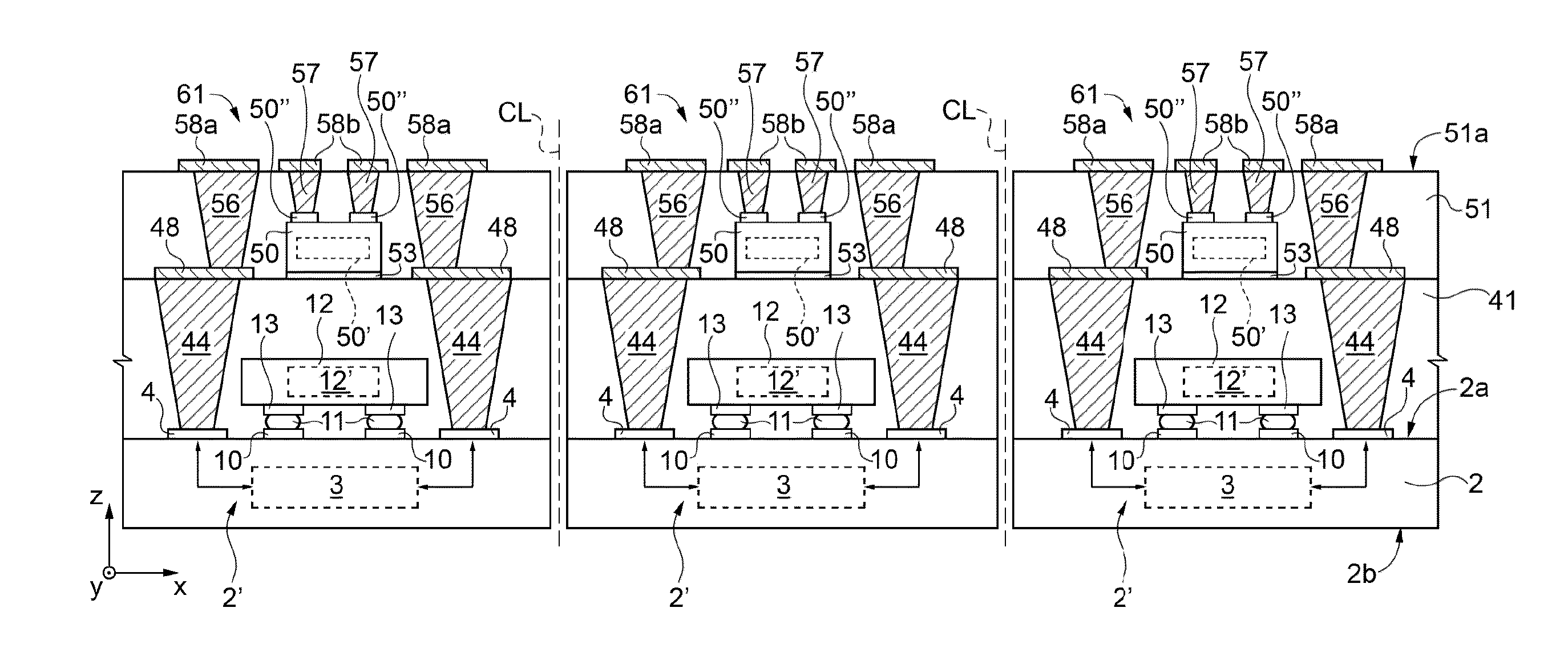
In the case of micromechanical structures with a membrane or the like (i.e., structures including further or different deformable elements), the necessary presence of a cavity means that a desired reduction of the resulting dimensions of the package is, however, difficult to obtain on account, for example, of the requisites of thickness of the walls of the cavity (which is frequently made of a composite substrate of the BT—bismaleimide triazine—type, having the function of covering structure).
Moreover, a marked reduction of the dimensions involves a greater difficulty in the steps of processing of the covering structure that closes the cavity at the top, and bigger problems linked to mismatches in the coefficients of thermal expansion of the materials used.
In general, there consequently arise problems of reliability and stability of performance, as the dimensions of the package decrease, which can jeopardize the usability of the resulting integrated devices.

Method used


Image

  • Wafer-level packaging of integrated devices, and manufacturing method thereof
  • Wafer-level packaging of integrated devices, and manufacturing method thereof
  • Wafer-level packaging of integrated devices, and manufacturing method thereof

Examples


Embodiment Construction

[0004]Within the field of integrated devices there is a desire to reduce the dimensions in order to meet increasingly stringent specifications of miniaturization, in particular in the field of portable apparatuses, such as, for example, smartphones, tablets, or personal digital assistants (PDAs).

[0005]In a known way, a MEMS integrated device generally comprises a first body (usually defined as “die”), which includes semiconductor material (in particular silicon), integrating a micromechanical structure, operating, for example, as a sensor for detecting one or more quantities (for example, for providing an accelerometer, or gyroscope, or magnetometer) and generates an electrical quantity that is a function of the quantity to be detected (for example, a capacitive variation, a variation of electrical resistance, etc.). In an equally known way, the die is the result of an operation of sawing, or singulation, of a wafer, where a plurality of elementary devices are simultaneously produce...


PUM

PropertyMeasurementUnit
separation distanceaaaaaaaaaa
electrical-aaaaaaaaaa
conductiveaaaaaaaaaa

Abstract

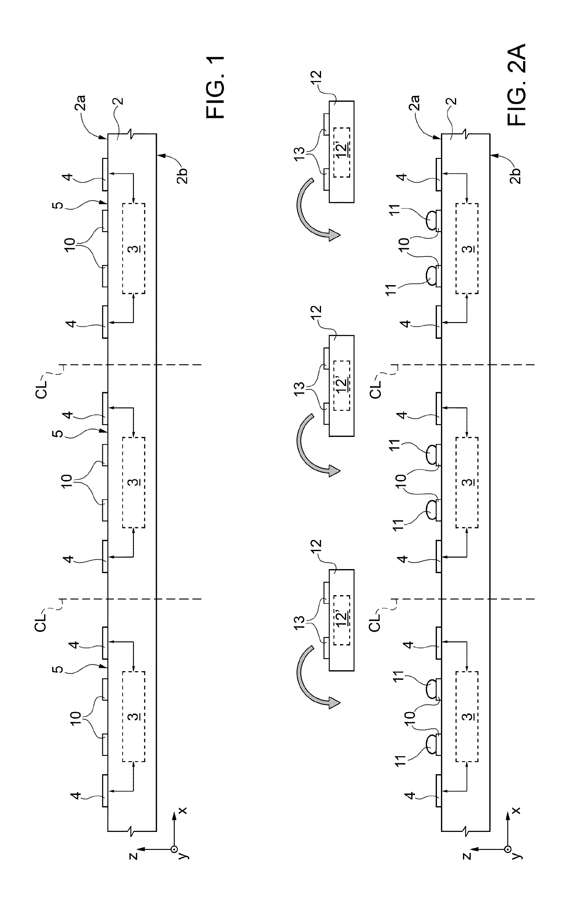
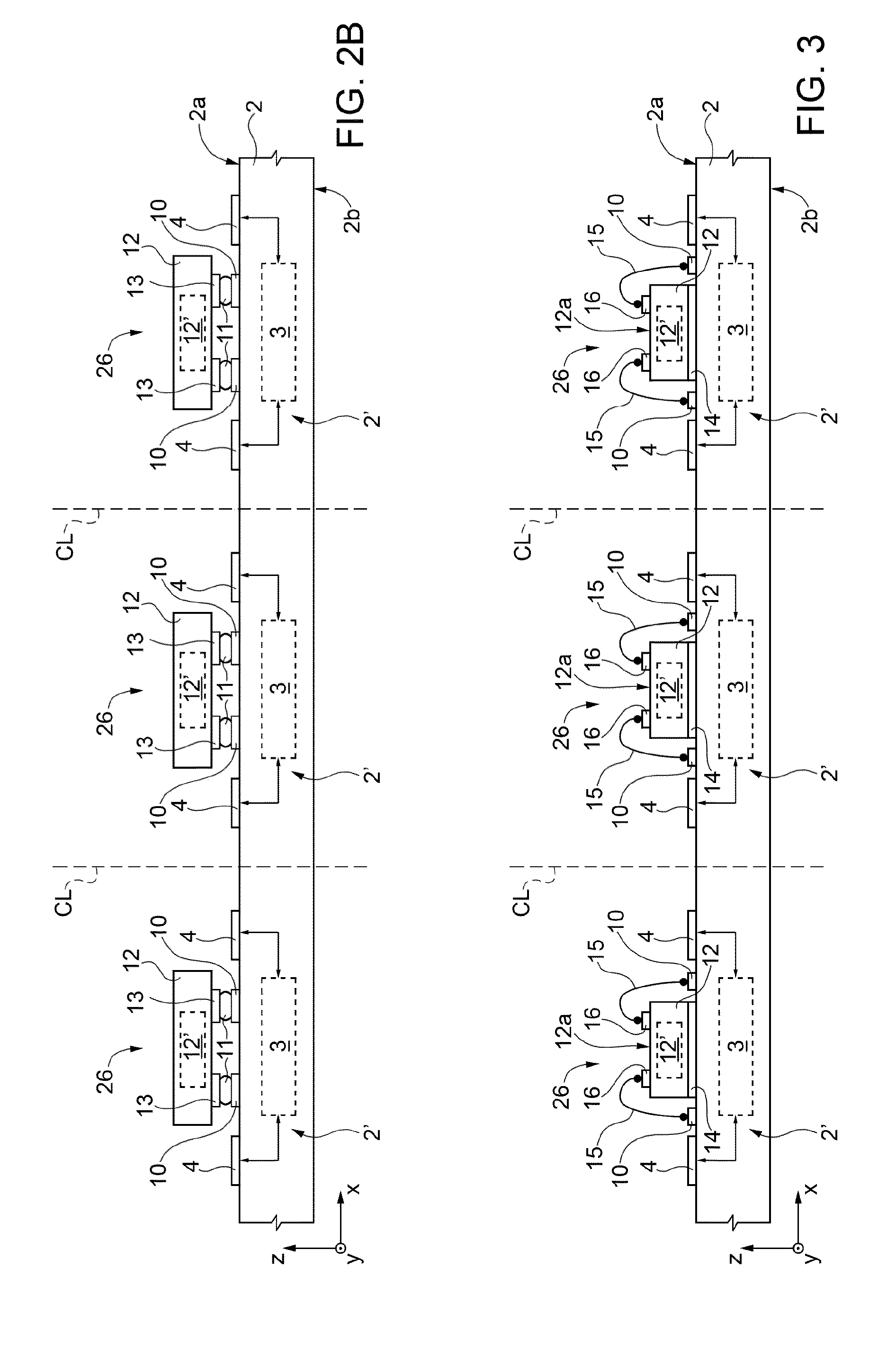
A wafer-level packaging, comprising: a first semiconductor body integrating a MEMS structure; a second semiconductor body, including a surface electrical-contact region and an ASIC coupled to the MEMS structure and to said electrical-contact region; a first coating layer, made of resin, which englobes and protects the first body, the second body, and the electrical-contact region; at least one first conductive through via, which extends through the first coating layer in an area corresponding, and electrically coupled, to the first electrical-contact region; an electrical-contact pad, which extends over the first coating layer, electrically coupled to the first conductive through via; a third semiconductor body, integrating an electronic circuit, glued on the first coating layer; a second coating layer, made of resin, which englobes and protects the third body; at least one second conductive through via, which extends completely through the second coating layer in an area corresponding, and electrically coupled, to the electrical-contact pad; and a further electrical-contact pad electrically coupled to the second conductive through via.

Description

BACKGROUND[0001]1. Technical Field[0002]The present disclosure relates to a wafer-level packaging of a plurality of integrated devices, such as, for example, microelectromechanical devices (MEMS) and / or electronic devices. The present disclosure moreover relates to a method for manufacturing said wafer-level packaging.[0003]2. Detailed Description[0004]Within the field of integrated devices there is a desire to reduce the dimensions in order to meet increasingly stringent specifications of miniaturization, in particular in the field of portable apparatuses, such as, for example, smartphones, tablets, or personal digital assistants (PDAs).[0005]In a known way, a MEMS integrated device generally comprises a first body (usually defined as “die”), which includes semiconductor material (in particular silicon), integrating a micromechanical structure, operating, for example, as a sensor for detecting one or more quantities (for example, for providing an accelerometer, or gyroscope, or mag...

Claims


Application Information

Patent Timeline
Patent Type & Authority Applications(United States)
IPC IPC(8): B81C1/00B81B7/00B81B3/00
CPCB81B7/007B81B3/0094B81C2203/00B81B2207/07B81C1/00301B81B2207/012B81C2203/0136H01L2225/06506H01L24/94H01L23/3114B81C1/00238H01L2224/73265H01L2224/81005H01L2224/97H01L24/97H01L25/50B81B2207/095H01L2224/94H01L2225/06513H01L2225/06524H01L2225/06548H01L21/561H01L2224/16145B81C2203/0792B81B2207/097H01L2224/32145H01L2224/48145H01L25/0657H01L2924/181H01L2924/12042H01L24/73H01L2224/04105H01L2224/32225H01L2224/73267H01L2924/18161H01L2924/18162H01L2224/85H01L2224/83H01L2224/81H01L2924/00012H01L2924/00H01L29/84
Inventor FORMOSA, KEVINMAGGI, LUCA
Owner STMICROELECTRONICS INT NV
Learn More