
High Accuracy Design Based Classification

Active Publication Date: 2014-10-09
KLA TENCOR TECH CORP
View PDF4 Cites 23 Cited by
  • Summary
  • Abstract
  • Description
  • Claims
  • Application Information

AI Technical Summary

Benefits of technology

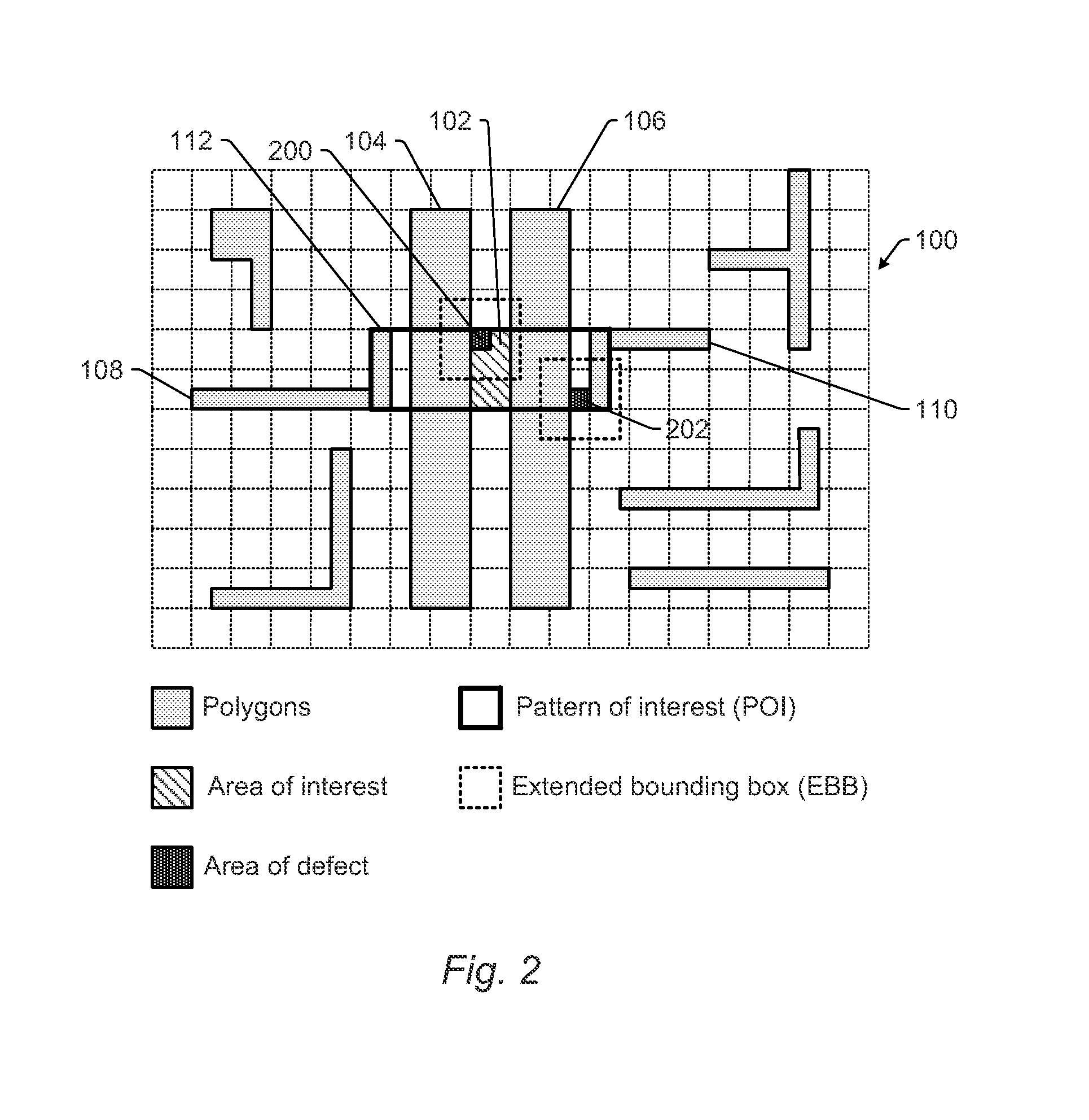
The patent describes a method for classifying defects on a wafer. It involves detecting a defect and creating a larger area around it called an extended bounding box. The extended bounding box is then dilated to create a larger area that includes polygons that match those in the detected defect. By analyzing the polygons in the dilated area, the method can determine if the defect is a hot spot or a non-hot spot. The system includes a computer system that performs this method and can automatically classify defects on a wafer. This helps in improving the efficiency and accuracy of defect detection and classification in the semiconductor industry.

Problems solved by technology

However, as the dimensions of semiconductor devices decrease, inspection becomes even more important to the successful manufacture of acceptable semiconductor devices because smaller defects can cause the devices to fail.
For instance, as the dimensions of semiconductor devices decrease, detection of defects of decreasing size has become necessary since even relatively small defects may cause unwanted aberrations in the semiconductor devices.
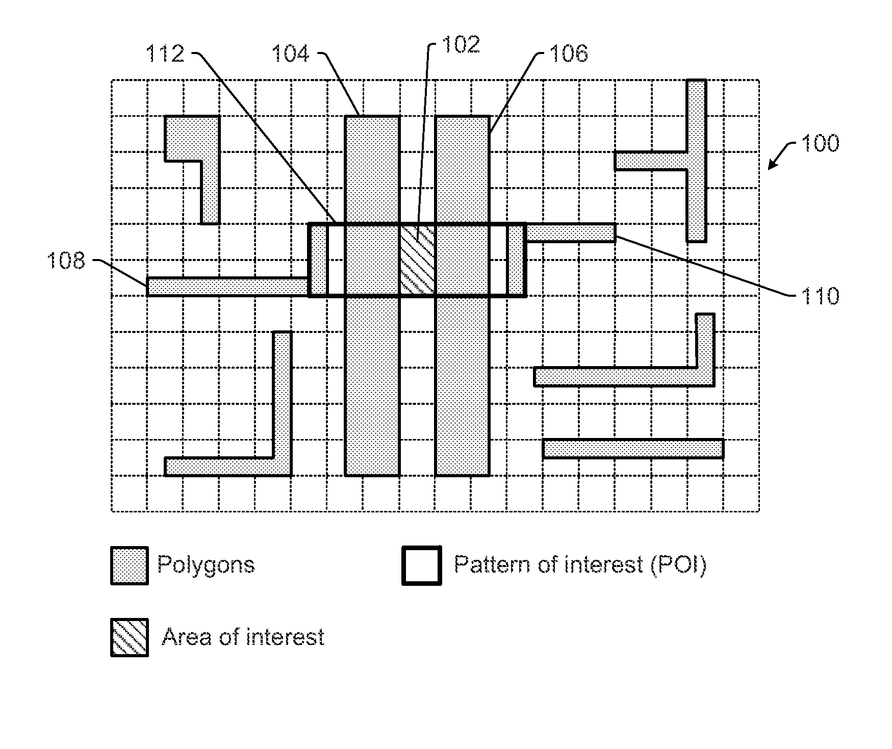
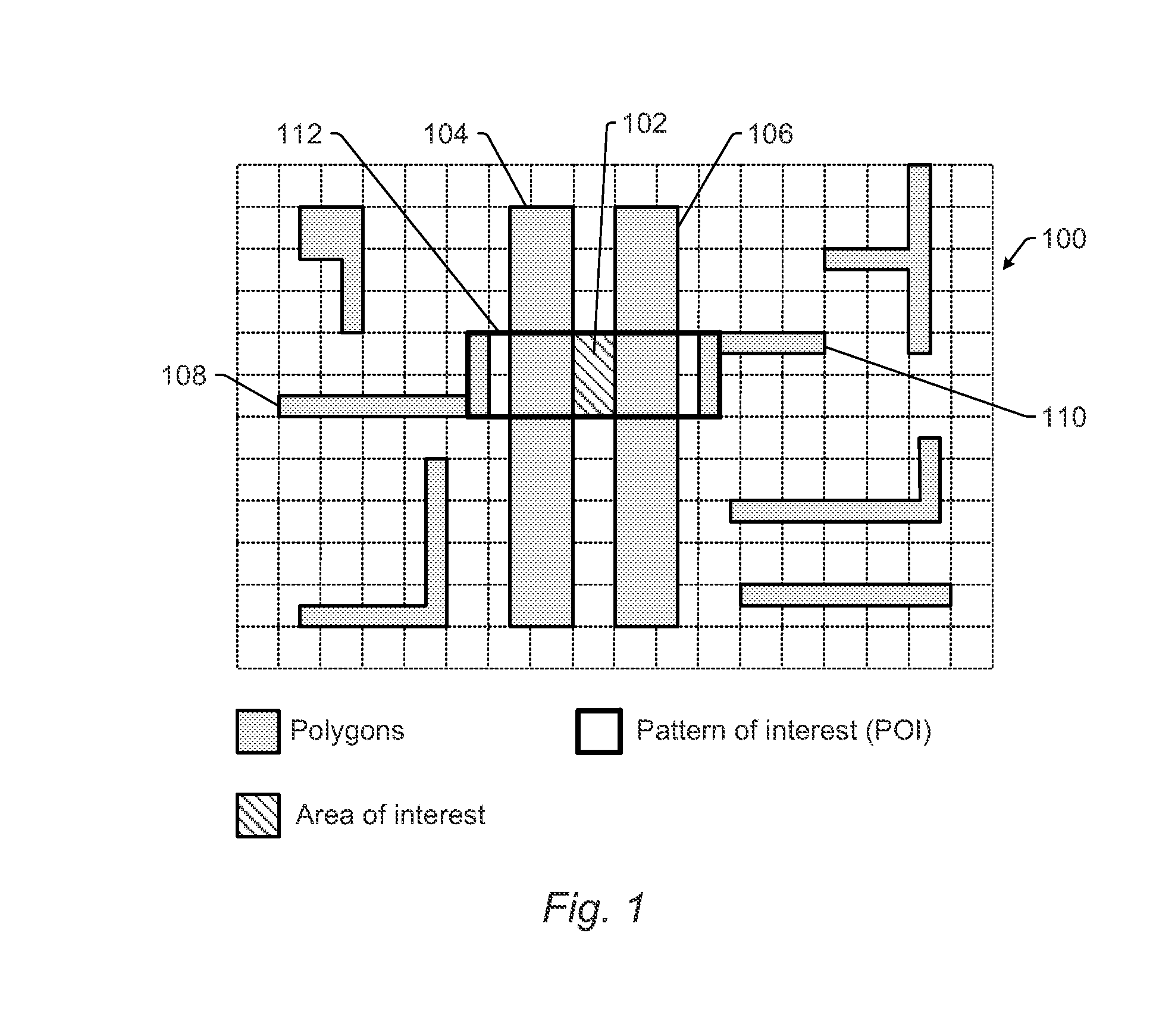
A design “hot spot” is a well-defined structure or rule within the design that has been identified as a relatively high risk for failure, either through simulations, defect inspection, or electrical testing.
This interaction can elevate the risk of failure at a particular location.
However, the coordinate accuracy of many modern optical and scanning electron microscope (SEM) imaging tools can often be smaller than the bounds of the hot spots.
When current methods for identifying whether a defect belongs to a hot spot are applied to one of these modern tools, it effectively negates the advantages provided by the improved coordinate accuracy of these tools.

Method used


Image

  • High Accuracy Design Based Classification
  • High Accuracy Design Based Classification
  • High Accuracy Design Based Classification

Examples


Embodiment Construction

[0021]Turning now to the drawings, it is noted that the figures are not drawn to scale. In particular, the scale of some of the elements of the figures is greatly exaggerated to emphasize characteristics of the elements. It is also noted that the figures are not drawn to the same scale. Elements shown in more than one figure that may be similarly configured have been indicated using the same reference numerals. Unless otherwise noted herein, any of the elements described and shown may include any suitable commercially available elements.

[0022]One embodiment relates to a method for classifying defects detected on a wafer. The embodiments described herein provide improved hot spot defect identification and take full advantage of the improved defect coordinate accuracy that inspection tools can provide. Therefore, the embodiments described herein can have a direct positive impact on the effectiveness of defect inspection in monitoring known hot spots and consequently on yield for semic...


PUM


Abstract

Systems and methods for classifying defects on a wafer are provided. One method includes dilating an extended bounding box (EBB) surrounding a defect position on a wafer in two dimensions in proportion to a width and height of a pattern of interest (POI) for a hot spot closest to the defect position. The method also includes determining if polygons in the POI match polygons in the dilated bounding box. If the polygons in the POI do not match the polygons in the dilated bounding box, the defect is classified as a non-hot spot defect. If the polygons in the POI match the polygons in the dilated bounding box, the defect is classified as a hot spot defect if the area of the EBB intersects the area of interest associated with the hot spot and a non-hot spot defect if the EBB area does not intersect the area of interest.

Description

BACKGROUND OF THE INVENTION[0001]1. Field of the Invention[0002]The present invention generally relates to systems and methods for classifying defects detected on a wafer.[0003]2. Description of the Related Art[0004]The following description and examples are not admitted to be prior art by virtue of their inclusion in this section.[0005]Inspection processes are used at various steps during a semiconductor manufacturing process to detect defects on wafers to promote higher yield in the manufacturing process and thus higher profits. Inspection has always been an important part of fabricating semiconductor devices such as ICs. However, as the dimensions of semiconductor devices decrease, inspection becomes even more important to the successful manufacture of acceptable semiconductor devices because smaller defects can cause the devices to fail. For instance, as the dimensions of semiconductor devices decrease, detection of defects of decreasing size has become necessary since even rela...

Claims


Application Information

Patent Timeline
IPC IPC(8): G06T7/00
CPCG06T7/0004G06T2207/10061G06T2207/30148
Inventor RAMACHANDRAN, VIJAYAKUMAR
Owner KLA TENCOR TECH CORP
Learn More