Detecting Defects on a Wafer

a technology of defects and wafers, applied in the field of detecting defects on wafers, can solve the problems of not leveraging the output generated by the inspection system at the pixel level, and the need to detect defects of decreasing siz

Active Publication Date: 2014-09-18
KLA TENCOR TECH CORP
View PDF10 Cites 23 Cited by
  • Summary
  • Abstract
  • Description
  • Claims
  • Application Information

AI Technical Summary

Benefits of technology

[0014]FIG. 1 is a block diagram illustrating one embodiment of a non-transitory computer-readable medium storing program instructions executable on a computer system for performing one or more of the method embodiments described herein; and

Problems solved by technology

However, as the dimensions of semiconductor devices decrease, inspection becomes even more important to the successful manufacture of acceptable semiconductor devices because smaller defects can cause the devices to fail.
For instance, as the dimensions of semiconductor devices decrease, detection of defects of decreasing size has become necessary since even relatively small defects may cause unwanted aberrations in the semiconductor devices.
Such previously used inspection methods, therefore, do not leverage the output generated by the inspection system at the pixel level, but rather combine the results at the wafer map level as the final result.

Method used


Image

  • Detecting Defects on a Wafer
  • Detecting Defects on a Wafer

Examples


Embodiment Construction

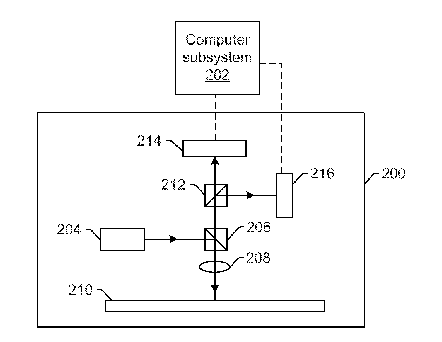
[0017]Turning now to the drawings, it is noted that the figures are not drawn to scale. In particular, the scale of some of the elements of the figures is greatly exaggerated to emphasize characteristics of the elements. It is also noted that the figures are not drawn to the same scale. Elements shown in more than one figure that may be similarly configured have been indicated using the same reference numerals. Unless otherwise noted herein, any of the elements described and shown may include any suitable commercially available elements.

[0018]One embodiment relates to a computer-implemented method for detecting defects on a wafer. The method includes determining difference values for pixels in first output for a wafer generated using a first optics mode of an inspection system. The first output may include any suitable output such as image signals or image data and may be generated as described further herein. The first optics mode and the inspection system may be configured as desc...


PUM


Abstract

Methods and systems for detecting defects on a wafer are provided. One method includes determining difference values for pixels in first output for a wafer generated using a first optics mode of an inspection system and determining other values for pixels in second output for the wafer generated using a second optics mode of the inspection system. The first and second optics modes are different from each other. The method also includes generating a two-dimensional scatter plot of the difference values and the other values for the pixels in the first and second output corresponding to substantially the same locations on the wafer. The method further includes detecting defects on the wafer based on the two-dimensional scatter plot.

Description

BACKGROUND OF THE INVENTION[0001]1. Field of the Invention[0002]This invention generally relates to detecting defects on a wafer. Certain embodiments relate to detecting defects on a wafer using a two-dimensional scatter plot generated from output generated by different optics modes of an inspection system.[0003]2. Description of the Related Art[0004]The following description and examples are not admitted to be prior art by virtue of their inclusion in this section.[0005]Inspection processes are used at various steps during a semiconductor manufacturing process to detect defects on wafers to promote higher yield in the manufacturing process and thus higher profits. Inspection has always been an important part of fabricating semiconductor devices such as ICs. However, as the dimensions of semiconductor devices decrease, inspection becomes even more important to the successful manufacture of acceptable semiconductor devices because smaller defects can cause the devices to fail. For in...

Claims


Application Information

Patent Timeline
Patent Type & Authority Applications(United States)
IPC IPC(8): G06T7/00
CPCG06T7/0004G06T2207/20076G06T2207/30148G06T7/001G06T2207/10061G01N21/9501G01N21/956G01N2021/8825G01N21/95607G01N21/8803G06T7/0002G01N21/88
Inventor HUANG, JUNQINGGAO, LISHENG
Owner KLA TENCOR TECH CORP
Why Eureka
Try Eureka