Organic electroluminescent element
a technology of electroluminescent elements and organic materials, which is applied in the direction of thermoelectric devices, solid-state devices, organic chemistry, etc., can solve the problems of reducing the efficiency of film-formation process, reducing the efficiency of conventional charge-generating layers, and shortened life, so as to achieve low driving voltage, suppress current leakage between pixels, and high luminous efficiency
- Summary
- Abstract
- Description
- Claims
- Application Information
AI Technical Summary
Benefits of technology
Problems solved by technology
Method used
Image

Examples
example 1
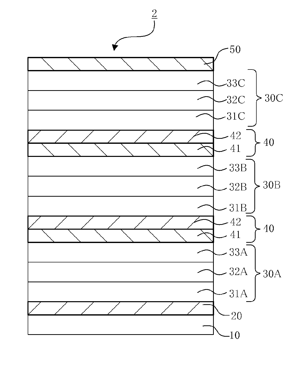
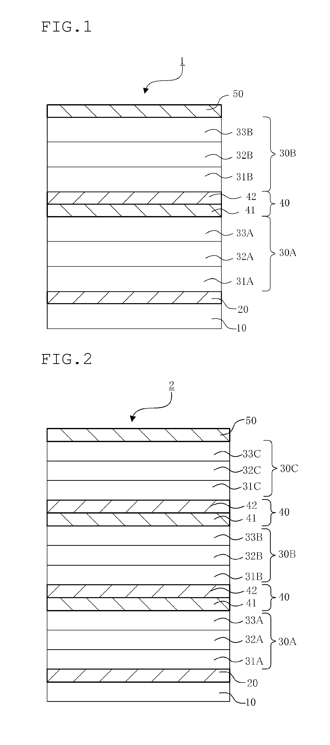
[0202]A bottom-emission type organic EL device in which emission is outcoupled from the substrate having the layer structure shown in FIG. 1 was fabricated. The structures of the organic compounds used in Example 1 are shown below. The compounds (P1) to (P4), which were compounds used in the P layer of the charge-transporting layer, were synthesized by referring to WO2010 / 064655 and WO2009 / 011327.
[0203]On a glass substrate having a dimension of 30 mm×30 mm, ITO was formed in a thickness of 240 nm as an anode. Subsequently, by deposition of SiO2, a cell for an organic EL device in which other parts than emitting regions of 2 mm×2 mm are masked by an insulating film (not shown) was fabricated.
[0204]On the anode, as the hole-injecting layer, hexanitrileazatriphenylene (HAT) having the above-mentioned structure was formed in a thickness of 10 nm.
[0205]On the hole-injecting layer, a blue emitting unit (first emitting unit) formed of a hole-transporting layer, a blue-emitting layer and an...
example 2
[0212]An organic EL device was fabricated in the same manner as in Example 1, except that a compound represented by the following formula (P2) was used instead of the compound represented by the above formula (P1) as the material for the P layer.
example 3
[0213]An organic EL device was fabricated in the same manner as in Example 1, except that a compound represented by the following formula (P3) was used instead of the compound represented by the above formula (P1) as the material for the P layer.
PUM
| Property | Measurement | Unit |
|---|---|---|
| sublimation temperature | aaaaa | aaaaa |
| transmittance | aaaaa | aaaaa |
| work function | aaaaa | aaaaa |
Abstract
Description
Claims
Application Information
 - Generate Ideas
- Intellectual Property
- Life Sciences
- Materials
- Tech Scout
- Unparalleled Data Quality
- Higher Quality Content
- 60% Fewer Hallucinations
Browse by: Latest US Patents, China's latest patents, Technical Efficacy Thesaurus, Application Domain, Technology Topic, Popular Technical Reports.
© 2025 PatSnap. All rights reserved.Legal|Privacy policy|Modern Slavery Act Transparency Statement|Sitemap|About US| Contact US: help@patsnap.com