Defect pattern evaluation method, defect pattern evaluation apparatus, and recording media

a defect pattern and evaluation method technology, applied in the direction of individual semiconductor device testing, semiconductor/solid-state device testing/measurement, instruments, etc., can solve the problem of difficulty in accurately extracting a pattern with a small number of detected defects

Active Publication Date: 2014-07-17
KIOXIA CORP
View PDF3 Cites 9 Cited by
  • Summary
  • Abstract
  • Description
  • Claims
  • Application Information

AI Technical Summary

Benefits of technology

The patent text describes a method and apparatus for evaluating defects in semiconductor devices. The method involves detecting defects on a patterned substrate and classifying them based on their type. The apparatus includes a defect inspection system and a scanning electron microscope. The technical effect of this invention is that it allows for accurate evaluation of small defects that may occur during semiconductor device manufacturing, even if they are not detected in large numbers. This is important for improving the manufacturing yield of semiconductor devices.

Problems solved by technology

Meanwhile, when patterns having a defect are lined up based on the number of patterns in which a defect is detected, it is difficult to accurately extract a pattern having a defect which is small in the detected number but. important.

Method used


Image

  • Defect pattern evaluation method, defect pattern evaluation apparatus, and recording media
  • Defect pattern evaluation method, defect pattern evaluation apparatus, and recording media
  • Defect pattern evaluation method, defect pattern evaluation apparatus, and recording media

Examples


Embodiment Construction

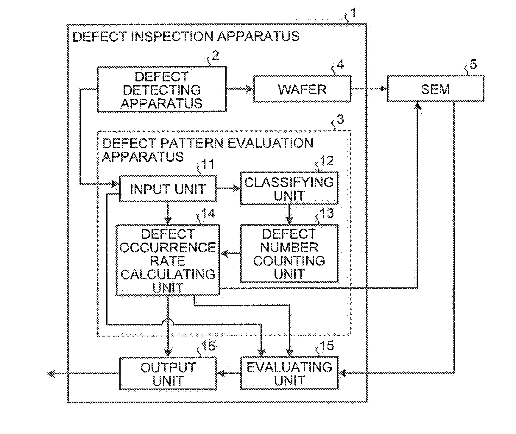
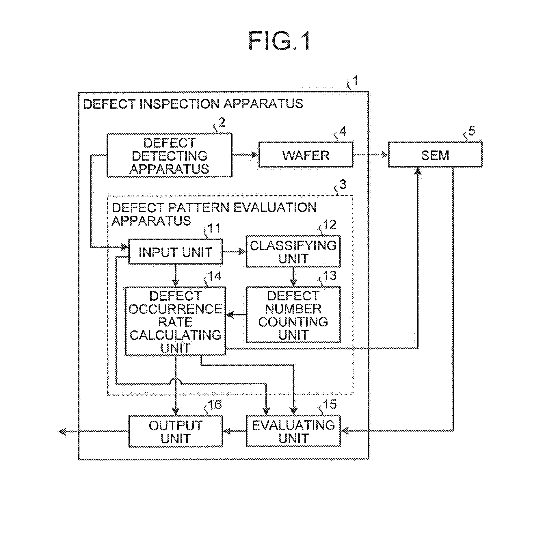
[0018]According to an embodiment, there is provided a defect pattern evaluation method. In the defect pattern evaluation method, defects are detected by performing optical defect inspection on a pattern on a substrate after a predetermined process for manufacturing a semiconductor device. Then, the defects are classified according to a type of a pattern layout using a pattern layout corresponding to coordinates of the defects.

[0019]Further, a computer calculates a defect occurrence rate by dividing the number of defects of each pattern layout by an arrangement number of the pattern layouts in an inspection region. Then, the defect occurrence rate of each pattern layout is output as an evaluation result.

[0020]A defect pattern evaluation method, a defect pattern evaluation apparatus, and a recording media according to an embodiment will be described in detail with reference to the accompanying drawings. The present invention is not limited to the following embodiment.

[0021]FIG. 1 is a...


PUM


Abstract

According to a defect pattern evaluation method of an embodiment, defects are detected by performing optical defect inspection on a pattern on a substrate. Then, the defects are classified according to a type of a pattern layout using a pattern layout corresponding to coordinates of the defects. Further, a computer calculates a defect occurrence rate by dividing the number of defects of each pattern layout by an arrangement number of the pattern layouts in an inspection region. Then, the defect occurrence rate of each pattern layout is output as an evaluation result.

Description

CROSS-REFERENCE TO RELATED APPLICATIONS[0001]This application is based upon and claims the benefit of priority from U.S. Provisional Application No. 61 / 753,061, filed on Jan. 16, 2013; the entire contents of which are incorporated herein by reference.FIELD[0002]Embodiments described herein relate generally to a defect pattern evaluation method, a defect pattern evaluation apparatus, and a recording media.BACKGROUND[0003]When semiconductor devices are manufactured, in order to improve a manufacturing yield of semiconductor devices, pattern defect inspection is performed after a predetermined process such as the lithography. The pattern defects are classified into random defects caused by device dust and systematic defects caused depending on the type of a pattern.[0004]In order to evaluate the systematic defects, patterns having a defect are first classified according to the type. At this time, a method such as design based binning (DEE) may be used as a pattern classifying method. I...

Claims


Application Information

Patent Timeline
IPC IPC(8): G01N21/956H01J37/26
CPCG01N21/956H01L22/12H01J37/26H01J2237/24592H01J2237/2817H01L22/20
Inventor MIYOSHI, SEIROARITAKE, TOSHIYUKI
Owner KIOXIA CORP
Why Eureka
Try Eureka