Semiconductor device structure for ohmic contact and method for fabricating the same

a technology of ohmic contact and semiconductor device, which is applied in the direction of semiconductor devices, basic electric elements, electrical equipment, etc., can solve the problems of shortened lifespan and deterioration of semiconductor devices, and achieve the effect of maintaining operating characteristics and improving the lifespan of semiconductor devices

Inactive Publication Date: 2014-07-03
HYUNDAI MOTOR CO LTD
View PDF2 Cites 3 Cited by
  • Summary
  • Abstract
  • Description
  • Claims
  • Application Information

AI Technical Summary

Benefits of technology

The present patent aims to prevent the diffusion of metal from the pad layer to the ohmic contact layer in a semiconductor device. This is achieved by adding an anti-diffusion layer between the two layers. The technical effect of this is that it improves the lifespan of the semiconductor device by maintaining its operating characteristics.

Problems solved by technology

Accordingly, the characteristics of the semiconductor device are deteriorated, and its lifespan is shortened.

Method used


Image

  • Semiconductor device structure for ohmic contact and method for fabricating the same
  • Semiconductor device structure for ohmic contact and method for fabricating the same
  • Semiconductor device structure for ohmic contact and method for fabricating the same

Examples


Embodiment Construction

[0019]Exemplary embodiments of the present disclosure will be described in detail with reference to the attached drawings. The present disclosure may be modified in many different forms and should not be construed as being limited to the exemplary embodiments set forth herein. Rather, the exemplary embodiments of the present disclosure are provided so that this disclosure will be thorough and complete, and will fully convey the concept of the present disclosure to those skilled in the art.

[0020]In the drawings, the thickness of layers and regions may be exaggerated for clarity. In addition, when a layer is described to be formed on another layer or on a substrate, this means that the layer may be formed on the other layer or on the substrate, or a third layer may be interposed between the layer and the other layer or the substrate. Like numbers refer to like elements throughout the specification.

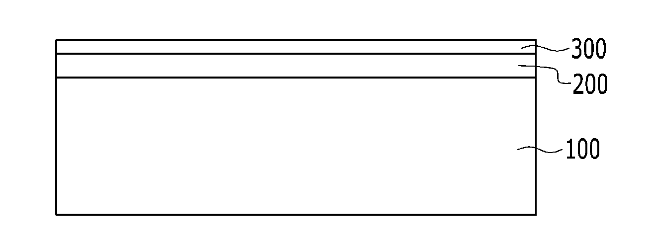
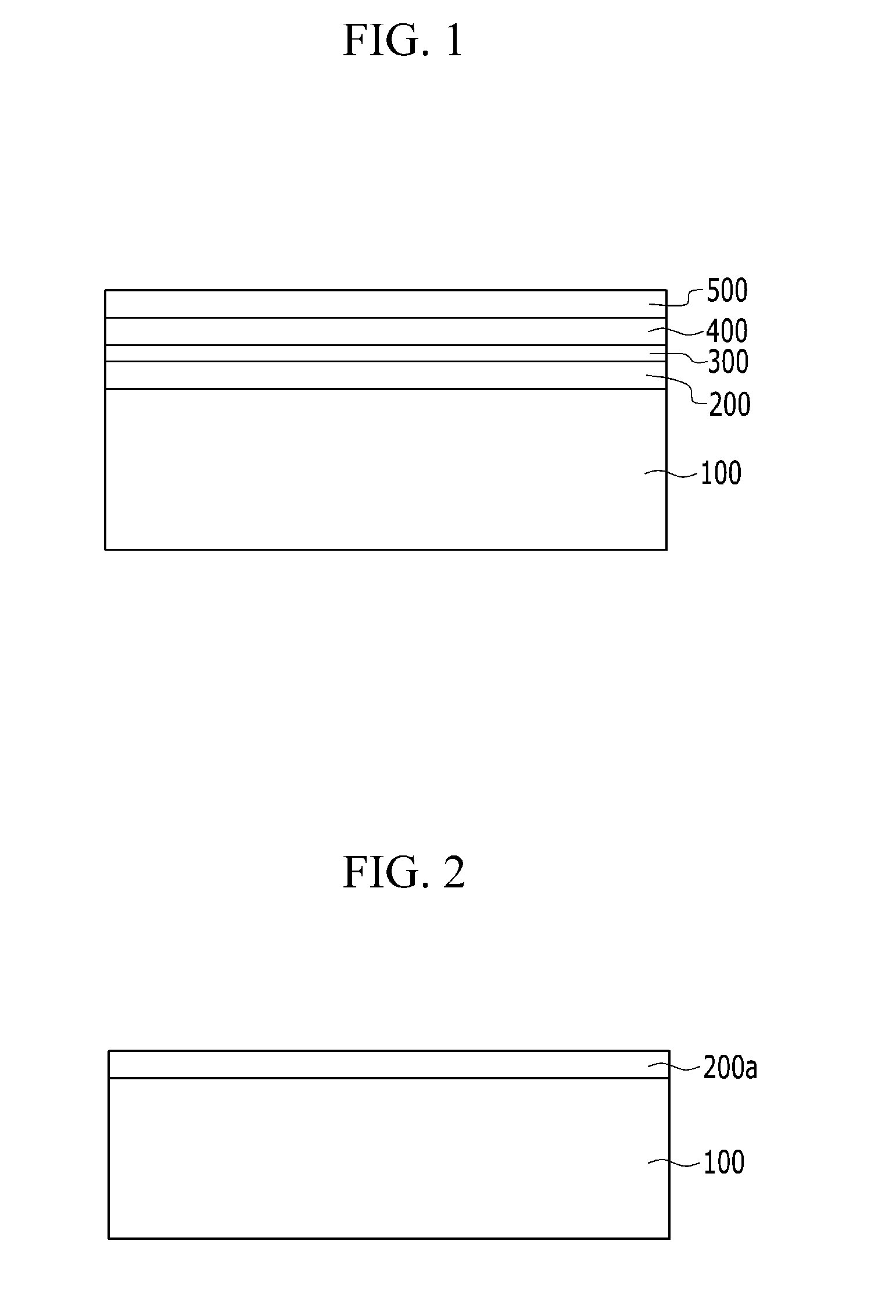
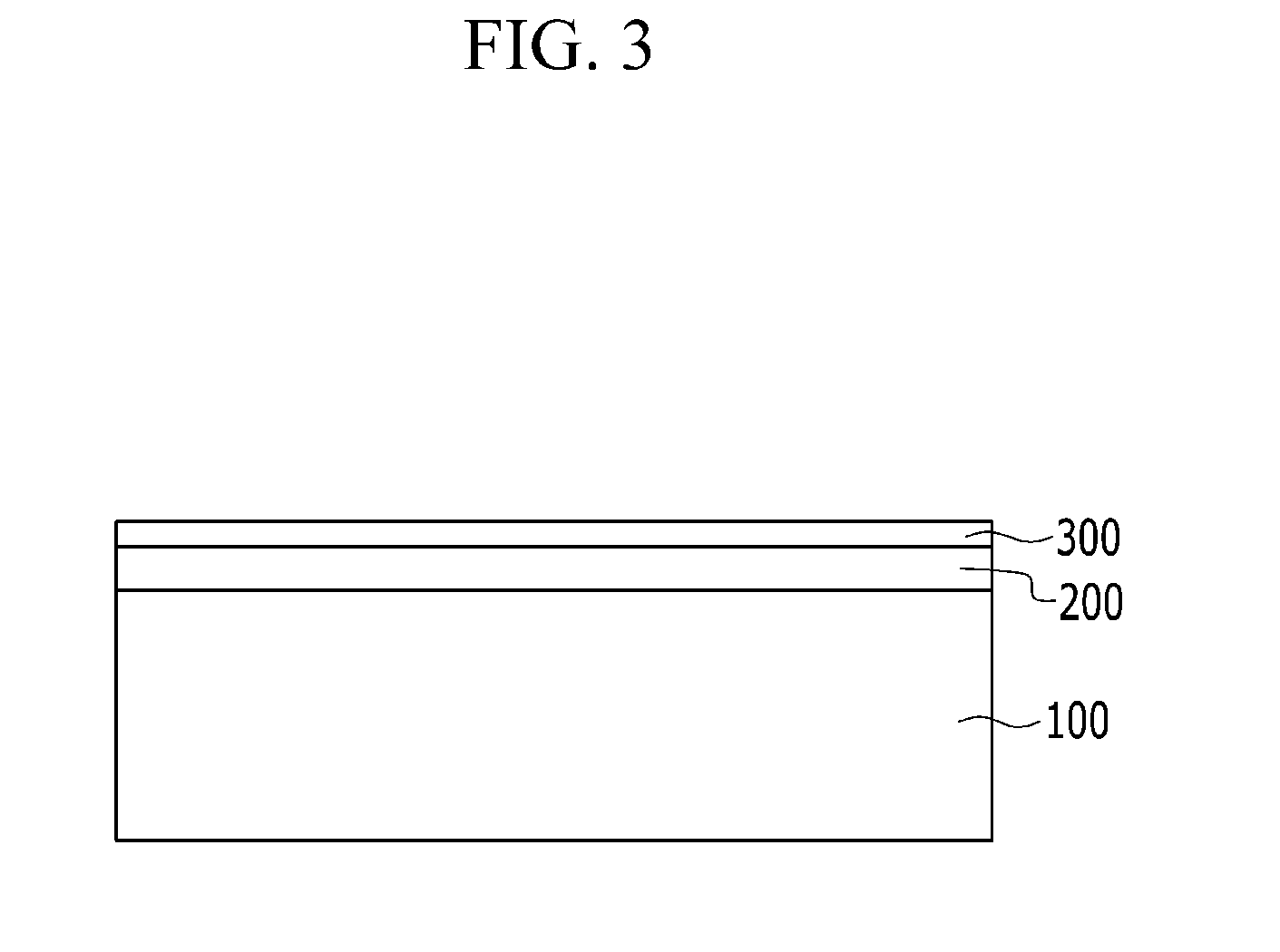
[0021]FIG. 1 is a cross-sectional view of a semiconductor device structure for an ohmic ...


PUM

PropertyMeasurementUnit
temperatureaaaaaaaaaa
breakdown voltageaaaaaaaaaa
current capacityaaaaaaaaaa

Abstract

A semiconductor device structure for an ohmic contact is provided, including a silicon carbide substrate and an ohmic contact layer disposed on the silicon carbide substrate. A carbon layer is disposed on the ohmic contact layer. An anti-diffusion layer is disposed on the carbon layer, and a pad layer is disposed on the anti-diffusion layer. The anti-diffusion layer is made of any one of tungsten (W), titanium (Ti), titanium nitride (TiN), tantalum (Ta), and tantalum nitride (TaN).

Description

CROSS-REFERENCE TO RELATED APPLICATION[0001]This application claims priority to and the benefit of Korean Patent Application No. 1 0-201 2-01 55376 filed in the Korean Intellectual Property Office on Dec. 27, 2012, the entire contents of which are incorporated herein by reference.TECHNICAL FIELD[0002]The present disclosure relates to a semiconductor device structure for an ohmic contact, and a method for fabricating the same.BACKGROUND[0003]With the recent trend toward large-sized and large-capacity application apparatuses, a power semiconductor device having a high breakdown voltage, a high current capacity, and high-speed switching characteristics has become necessary. A silicon carbide (SiC) power element is spotlighted as a device capable of meeting the above-mentioned characteristics due to its excellent characteristics compared to a conventional silicon (Si) device, and currently is actively being researched.[0004]In general, a silicon carbide power element includes an ohmic c...

Claims


Application Information

Patent Timeline
Patent Type & Authority Applications(United States)
IPC IPC(8): H01L29/45H01L21/28H01L29/16
CPCH01L29/45H01L29/1608H01L21/28H01L21/0485
Inventor KANG, SU BINHONG, KYOUNG-KOOKLEE, JONG SEOKJUNG, YOUNGKYUN
Owner HYUNDAI MOTOR CO LTD
Why Eureka
Try Eureka