High frequency switch circuit
a high-frequency switch and circuit technology, applied in electronic switching, pulse technique, semiconductor devices, etc., can solve the problems of conventional mosfet fabricated on low resistive silicon substrates that are not suitable for high-frequency switch circuits, failure to operate as switch circuits, and mosfet on conventional circuits, etc., to achieve high-performance switch circuits, low power consumption, and low cost.
- Summary
- Abstract
- Description
- Claims
- Application Information
AI Technical Summary
Benefits of technology
Problems solved by technology
Method used
Image


Examples
first embodiment
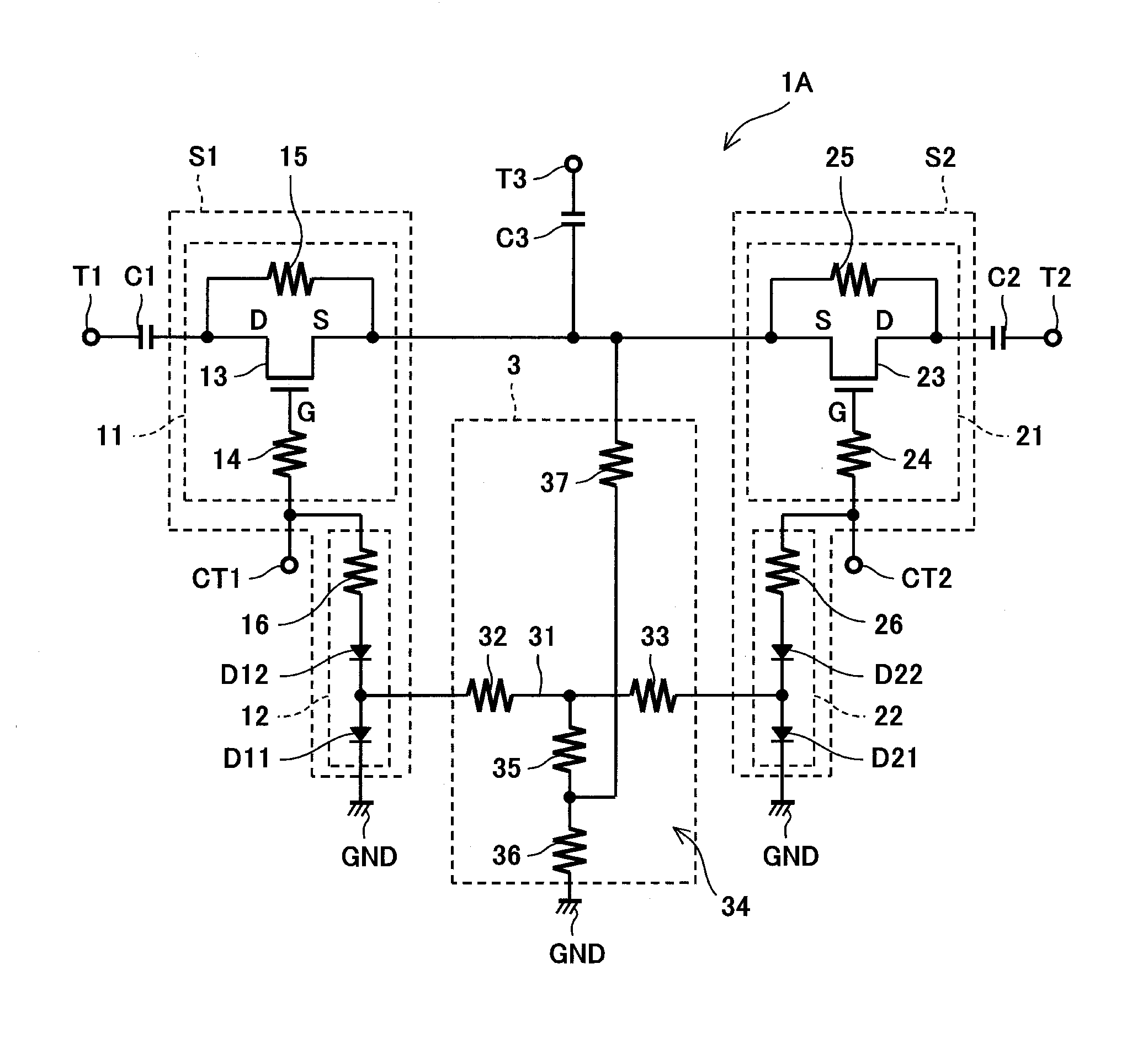
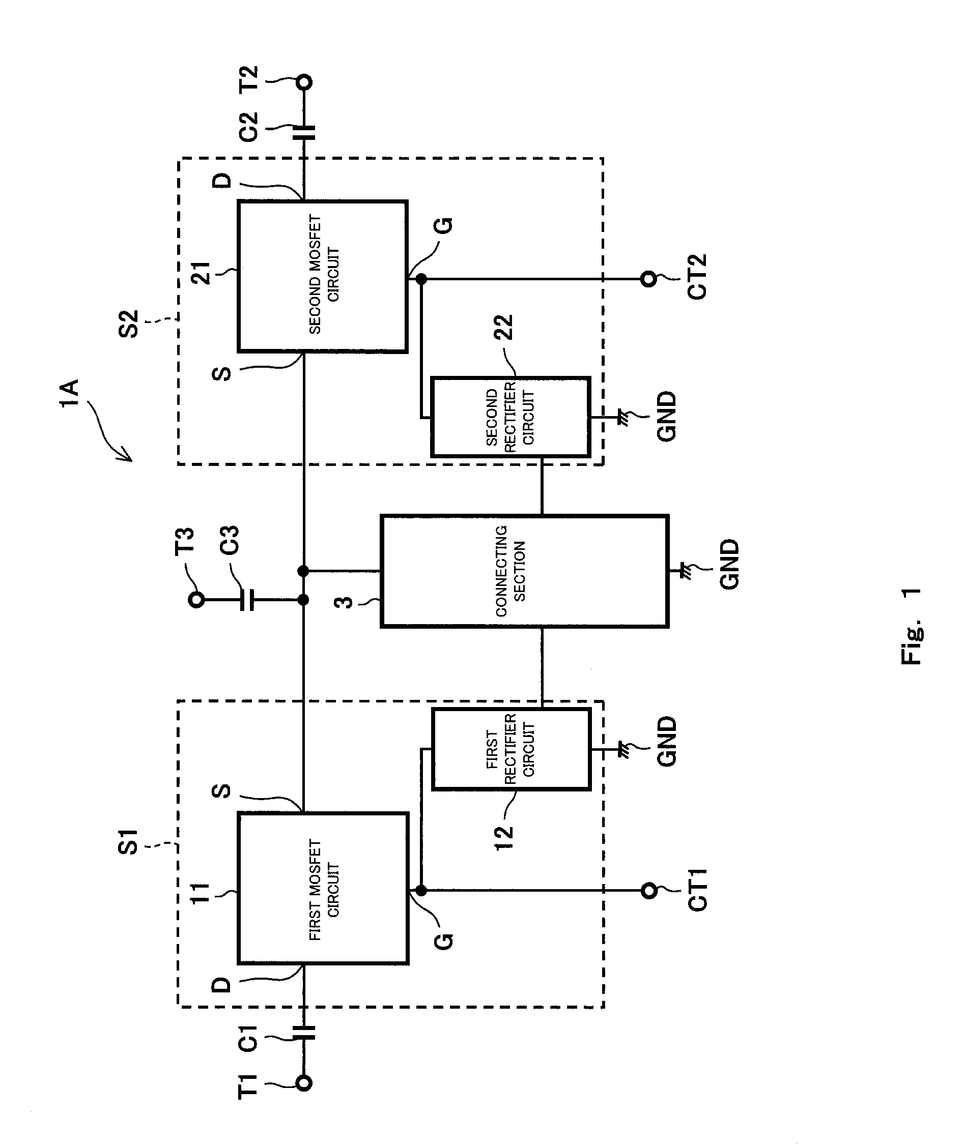
[0034]In the first place, a description will be given in regard to a high frequency switch circuit according to a first embodiment of the present invention. FIG. 1 is a circuit diagram showing a schematic configuration of a high frequency switch circuit according to the first embodiment of the present invention. As shown in FIG. 1, the switch circuit 1A of the present embodiment is configured as a high frequency switch circuit that makes use of a first control voltage VC1 applied to a first control terminal CT1 that controls the connection between a common signal terminal T3 and a first signal terminal T1 and / or a second control voltage VC2 applied to a second control terminal CT2 that controls the connection between the common signal terminal T3 and a second signal terminal T2, thereby to effect such switching between the first signal terminal T1 and the second signal terminal T2 that either one of the first signal terminal T1 and the second signal terminal T2 is selectively connec...
second embodiment
[0063]Next, a description will be given in regard to a high frequency switch circuit according to a second embodiment of the present invention. FIG. 4 is a circuit diagram showing a schematic configuration of a high frequency switch circuit according to the second embodiment of the present invention. In the present embodiment, the same reference numerals are used to refer to the same elements as the first embodiment, and their redundant description will be omitted accordingly. The switch circuit 1B of the second embodiment differs from the switch circuit 1A of the first embodiment in that the switch circuit 1B further includes at least one section (a third signal section S4 and a fourth signal section S5) having the same configuration as the second signal section S2 and which are provided for switching between the common signal terminal and at least one signal terminal (two signal terminals in the second embodiment, i.e., a third signal terminal T4 and a fourth signal terminal T5).
[...
third embodiment
[0066]Next, a description will be given in regard to a high frequency switch circuit according to a third embodiment of the present invention. FIG. 5 is a circuit diagram showing a schematic configuration of a high frequency switch circuit according to the third embodiment of the present invention. In the present embodiment, the same reference numerals are used to refer to the same components as the first embodiment, and their redundant description will be omitted accordingly. The difference of the switch circuit 1C of the present embodiment from the switch circuit 1A of the first embodiment is that it has, as a connecting section, a first connecting section 3C1 and a second connecting section 3C2. The first connecting section 3C1 establishes connection between the forward current input terminal side of at least one of the rectifier elements of the first rectifier circuit 12 and the first signal terminal T1 side (the drain terminal of the first MOSFET circuit 11 in the present embod...
PUM
 Abstract
Description
Claims
Application Information
 - R&D
- Intellectual Property
- Life Sciences
- Materials
- Tech Scout
- Unparalleled Data Quality
- Higher Quality Content
- 60% Fewer Hallucinations
Browse by: Latest US Patents, China's latest patents, Technical Efficacy Thesaurus, Application Domain, Technology Topic, Popular Technical Reports.
© 2025 PatSnap. All rights reserved.Legal|Privacy policy|Modern Slavery Act Transparency Statement|Sitemap|About US| Contact US: help@patsnap.com