Electronic writing system and operating method thereof
a writing system and electronic writing technology, applied in the field of electronic writing systems, can solve the problems of user inconvenience, high cost of electronic writing systems with large sizes of resistance type or capacitor types, and unfriendly design for users, and achieve the effect of reducing operation inconvenien
- Summary
- Abstract
- Description
- Claims
- Application Information
AI Technical Summary
Benefits of technology
Problems solved by technology
Method used
Image
Examples
first embodiment
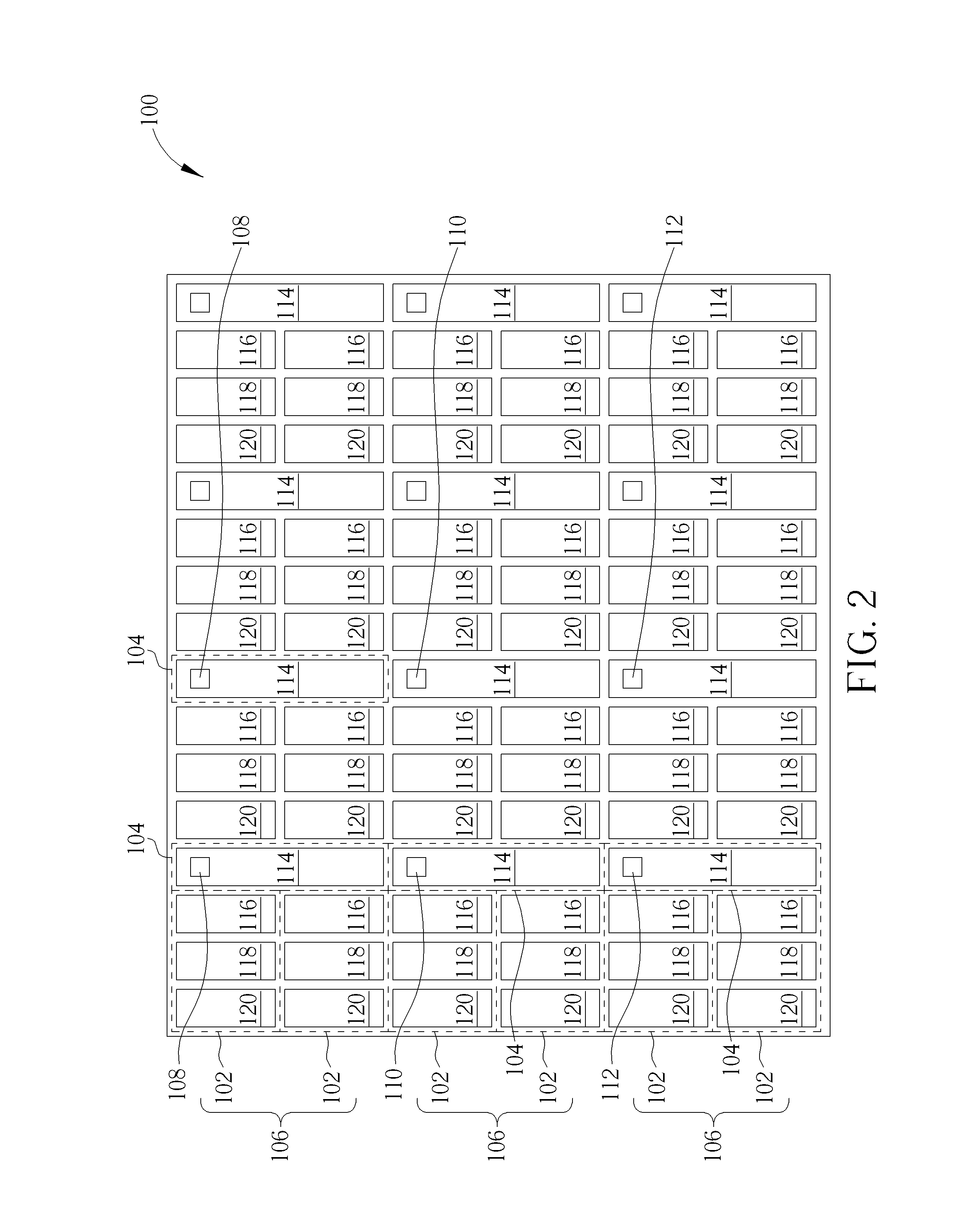
[0030]With reference to FIG. 3, FIG. 3 is a top-view schematic diagram of a display device of an electronic writing system according to a second preferred embodiment of the present disclosure. As shown in FIG. 3, in comparison with the display device of the first embodiment, each of the sensing regions 104 of the display device 200 of this embodiment is disposed in one of the fourth color filters 116 in its corresponding pixel region group 106, and each sensing region 104 does not have a transparent area. It should be noted that the fourth color filters 116 of this embodiment are blue color filters. Since human eyes have low sensitivity to blue light, disposing the sensing regions 104 in each fourth color filter 116 will not affect the color displayed by the display device 100 and can further effectively save the space for disposing the optical sensors in this embodiment.
[0031]In addition, based the aforementioned display device, the present disclosure further provides an image eras...
third embodiment
[0037]With reference to FIG. 7, FIG. 7 is a sectional schematic diagram of an image eraser of an electronic writing system according to a fourth preferred embodiment of the present disclosure. As shown in FIG. 7, in comparison with the third embodiment, the light entrance surface 314a and the light exit surface 314b of the LGP 314 are parallel with and face to each other in the image eraser 400 of this embodiment, which means the light entrance surface 314a is the bottom surface of the LGP 314 and the light source 320 is disposed between the holder 302 and the LGP 314. Furthermore, the bottom surface of the LGP 314 of this embodiment does not have micro structures, but not limited thereto.
[0038]With reference to FIG. 8, FIG. 8 is a sectional schematic diagram of an image eraser of an electronic writing system according to a fifth preferred embodiment of the present disclosure. As shown in FIG. 8, in comparison with the third embodiment, the image eraser 600 is a two-sided light-emit...
PUM
 Abstract
Description
Claims
Application Information
 - R&D
- Intellectual Property
- Life Sciences
- Materials
- Tech Scout
- Unparalleled Data Quality
- Higher Quality Content
- 60% Fewer Hallucinations
Browse by: Latest US Patents, China's latest patents, Technical Efficacy Thesaurus, Application Domain, Technology Topic, Popular Technical Reports.
© 2025 PatSnap. All rights reserved.Legal|Privacy policy|Modern Slavery Act Transparency Statement|Sitemap|About US| Contact US: help@patsnap.com


