
Pixel Arrangement Structure for Organic Light Emitting Diode Display

a light-emitting diode and organic technology, applied in the direction of discharge tube luminescnet screens, discharge tube/lamp details, electric discharge lamps, etc., can solve the problem of reducing the lifespan of the entire oled display, and achieve the effect of minimizing the overall aperture ratio

Active Publication Date: 2013-05-09
SAMSUNG DISPLAY CO LTD
View PDF1 Cites 38 Cited by
  • Summary
  • Abstract
  • Description
  • Claims
  • Application Information

AI Technical Summary

Benefits of technology

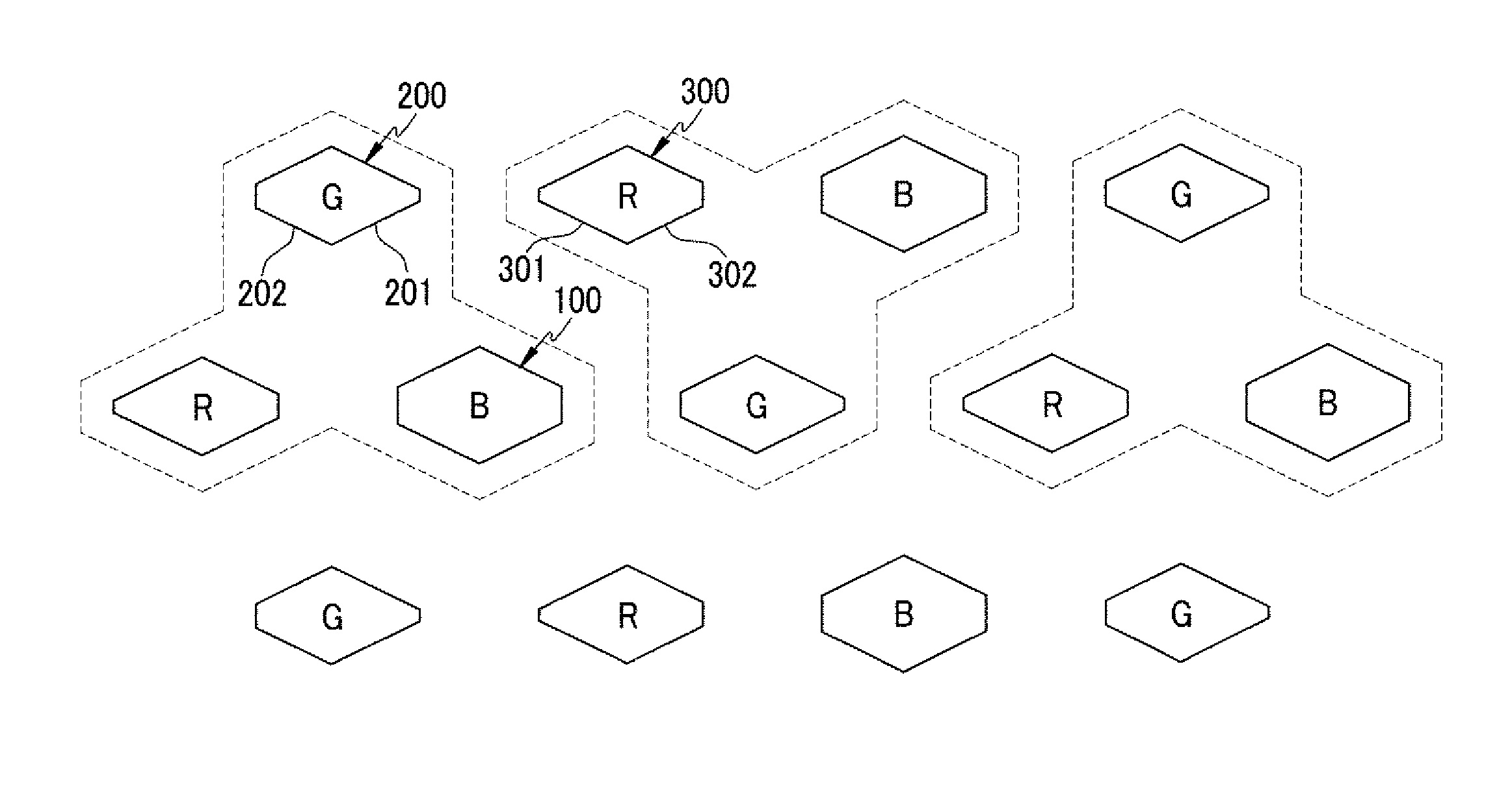
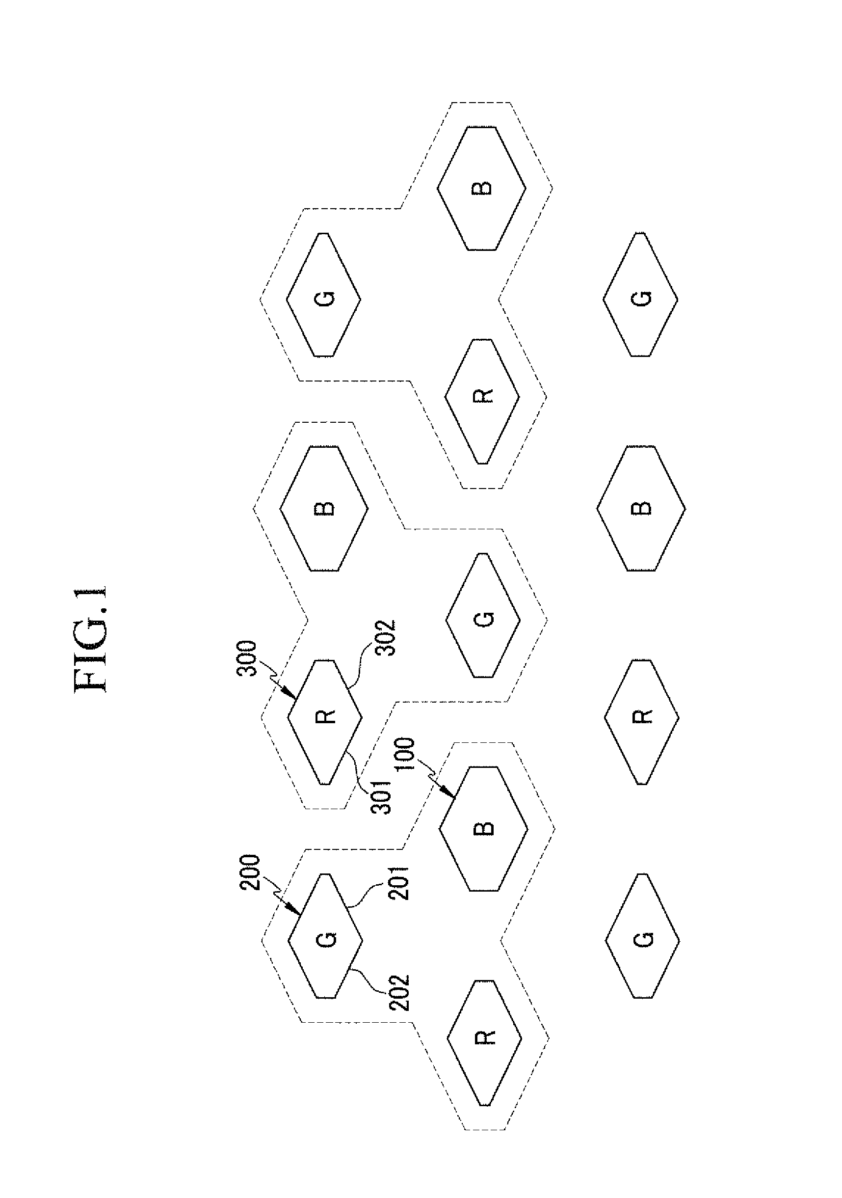
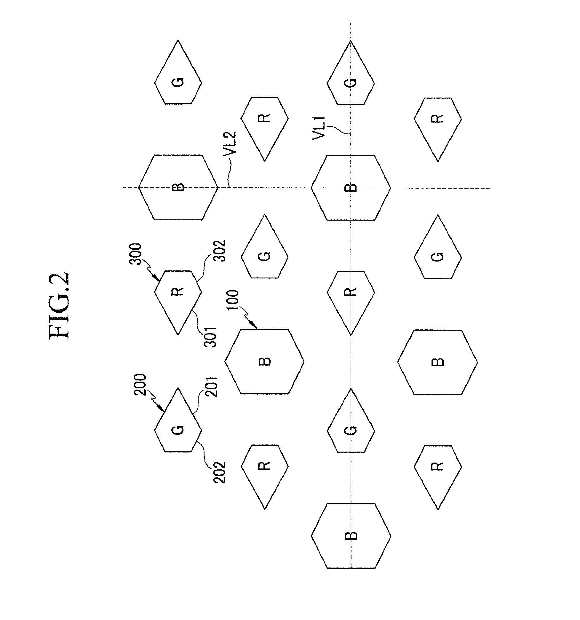
The present invention is a pixel structure for an organic light emitting diode display that minimizes the decrease in the overall aperture ratio while considering the lifespan of the organic layer. This means that the display's pixels are arranged in a way that allows for more light to escape while still keeping the organic layer alive for a longer time. This results in better image quality and a longer lifespan for the display.

Problems solved by technology

Since each of the pixels includes an organic layer emitting light of a different color, the organic layers emitting light of different colors are different in lifespan, which leads to a reduction in the lifespan of the entire OLED display.

Method used


Image

  • Pixel Arrangement Structure for Organic Light Emitting Diode Display
  • Pixel Arrangement Structure for Organic Light Emitting Diode Display
  • Pixel Arrangement Structure for Organic Light Emitting Diode Display

Examples


Embodiment Construction

[0026]The present invention will be described more fully hereinafter with reference to the accompanying drawings, in which exemplary embodiments of the invention are shown. As those skilled in the art will realize, the described embodiments may be modified in various different ways, all without departing from the spirit or scope of the present invention.

[0027]The drawings and description are to be regarded as illustrative in nature and not restrictive. Like reference numerals designate like elements throughout the specification.

[0028]Furthermore, the same constituent elements in exemplary embodiments are denoted by the same reference numerals and will be described representatively in a first exemplary embodiment, and only configurations different from those of the first exemplary embodiment will be described in the other exemplary embodiments.

[0029]The size and thickness of components shown in the drawings may be arbitrarily illustrated herein for better understanding and ease of de...


PUM


Abstract

A pixel arrangement structure for an organic light emitting diode display includes a first pixel, a second pixel and a third pixel. The first pixel has a larger area than the second pixel and the third pixel, and the first pixel, the second pixel and the third pixel have different planar shapes relative to each other.

Description

CLAIM OF PRIORITY[0001]This application makes reference to, incorporates the same herein, and claims all benefits accruing under 35 U.S.C. §119 from an application earlier filed in the Korean Intellectual Property Office on the 3 Nov. 2011 and there duly assigned Ser. No. 10-2011-0114027.BACKGROUND OF THE INVENTION[0002]1. Field of the Invention[0003]The present invention relates generally to a pixel arrangement structure for an organic light emitting diode display, and more particularly, to a pixel arrangement structure for an organic light emitting diode display in which a plurality of pixels emit light to display an image.[0004]2. Description of the Related Art[0005]As a display device which displays an image, an organic light emitting diode (OLED) display has come into the spotlight in recent years.[0006]The OLED display, unlike a liquid crystal display (LCD) device, has a self-luminous characteristic and does not need a separate light source, thereby reducing its thickness and ...

Claims


Application Information

Patent Timeline
Patent Type & Authority Applications(United States)
IPC IPC(8): H01J1/62
CPCH01L27/3218H01L27/3216H10K59/352H10K59/353H10K50/11H10K50/805
Inventor HONG, JAE-MIN
Owner SAMSUNG DISPLAY CO LTD
Learn More