Touch display device and manufacturing method thereof
a technology of touch display and manufacturing method, which is applied in the direction of thermoelectric devices, solid-state devices, instruments, etc., can solve the problem of large interference in signal detection, and achieve the effect of high touch detection accuracy
- Summary
- Abstract
- Description
- Claims
- Application Information
AI Technical Summary
Benefits of technology
Problems solved by technology
Method used
Image
Examples
first embodiment
The First Embodiment
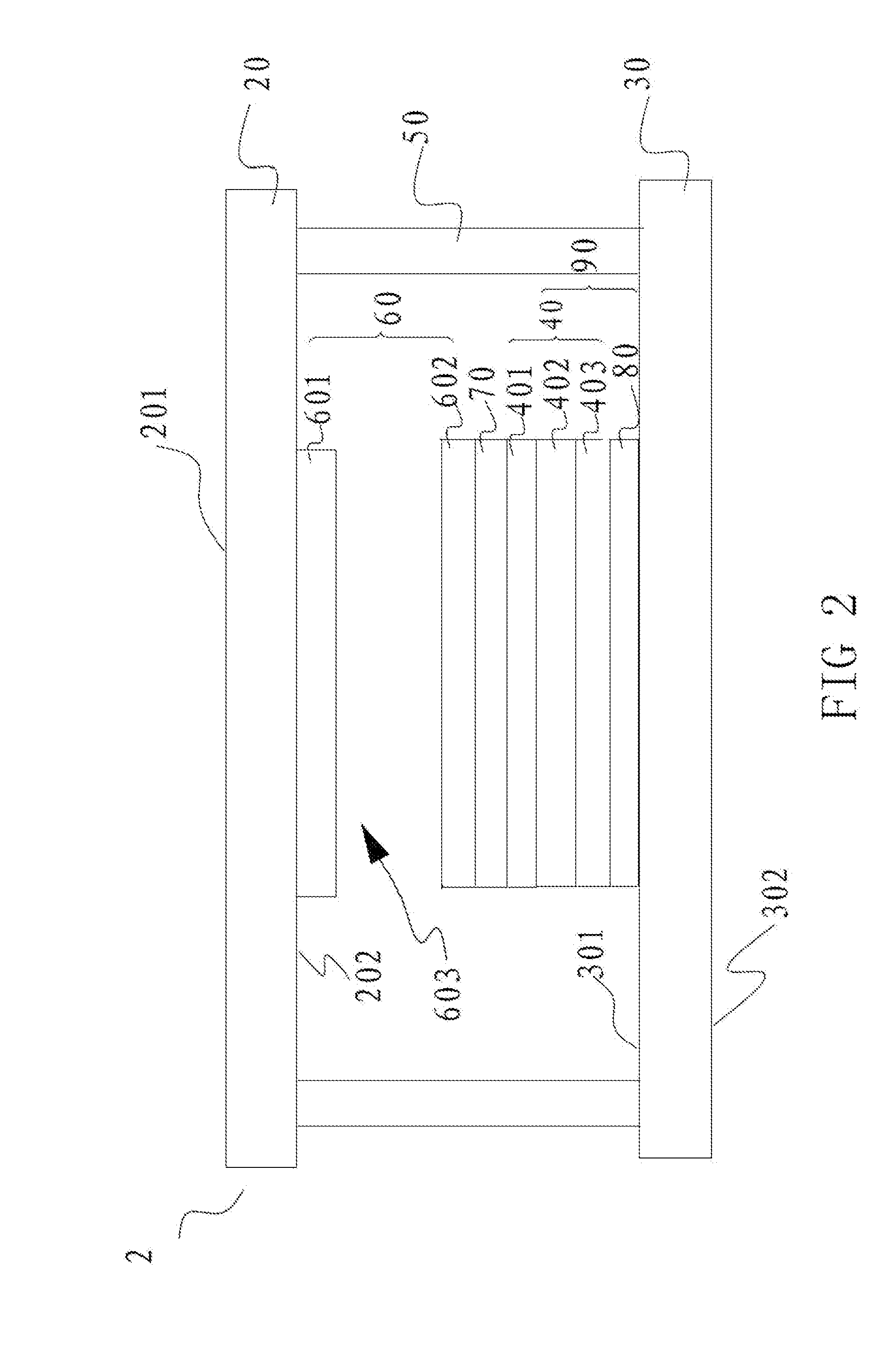
[0050]FIG. 2 is a schematic view of a touch display device in accordance with the first embodiment of the present invention. As shown in FIG. 2, a touch display device 2 in the present embodiment comprises an OLED display layer 90 disposed on a lower substrate 30; an upper substrate 20; an air layer 603 formed between the upper substrate 20 and the lower substrate 30; and a touch module 60 formed by a first sensing circuit layer 601 and a second sensing circuit layer 602, wherein he first sensing circuit layer and the second sensing circuit layer being spaced and the distance between them is more than 2 um.
[0051]The upper substrate 20 and the lower substrate 30 can be made of transparent materials, such as solid glass substrates and flexible plastic substrate. The upper substrate 20 comprises a first surface 201 away from the OLED display layer 90 and a second surface 202 close to the OLED display layer 90, wherein the first sensing circuit layer 601 is disposed ...
second embodiment
The Second Embodiment
[0064]FIG. 5 is a schematic view of a touch display device in accordance with a second embodiment of the present invention. The touch display device comprises: an upper substrate 20, a lower substrate 30, a protection layer 70, an OLED display layer 90 and a touch module 60. Components used in the present embodiment and the relative positions between the components are similar to the first embodiment; wherein the main difference lies in the position of the touch module 60 among other components. In the first embodiment, the air layer 603 is between the first sensing circuit layer 601 and the second sensing circuit layer 602, more specifically, the first sensing circuit layer 601 and the second sensing circuit layer 602 of the touch module 60 are located on the second surface 202 of the upper substrate 20 and above the OLED display layer 90 respectively and more particularly, the second sensing circuit layer 602 is disposed on a surface of the protection layer 70...
third embodiment
The Third Embodiment
[0065]FIG. 6 is a schematic view of a touch display device in accordance with the third embodiment of the present invention. Components used in the present embodiment and the relative positions between the components are similar to the first embodiment; the main difference lies in the position of the touch module 60 between other components, namely in the first embodiment, the air layer 603 is between the first sensing circuit layer 601 and the second sensing circuit layer 602, more specifically, the first sensing circuit layer 601 and the second sensing circuit layer 602 of the touch module 60 are disposed on the second surface 202 of the upper substrate 20 and on a surface of the protection layer 70 respectively. However, in the present embodiment, the upper substrate 20 is between the first sensing circuit layer 601 and the second sensing circuit layer 602, more specifically, the second sensing circuit layer 602 is disposed on the first surface 201 of the uppe...
PUM
 Abstract
Description
Claims
Application Information
 - R&D
- Intellectual Property
- Life Sciences
- Materials
- Tech Scout
- Unparalleled Data Quality
- Higher Quality Content
- 60% Fewer Hallucinations
Browse by: Latest US Patents, China's latest patents, Technical Efficacy Thesaurus, Application Domain, Technology Topic, Popular Technical Reports.
© 2025 PatSnap. All rights reserved.Legal|Privacy policy|Modern Slavery Act Transparency Statement|Sitemap|About US| Contact US: help@patsnap.com


