Touch Panel for Providing a Shield Against Noise
a technology of touch panel and shield, which is applied in the field of touch panel, can solve the problems that the conventional optical touch device cannot meet the requirements of ordinary portable lcds, and achieve the effect of preventing noise more effectively
- Summary
- Abstract
- Description
- Claims
- Application Information
AI Technical Summary
Benefits of technology
Problems solved by technology
Method used
Image

Examples
first embodiment
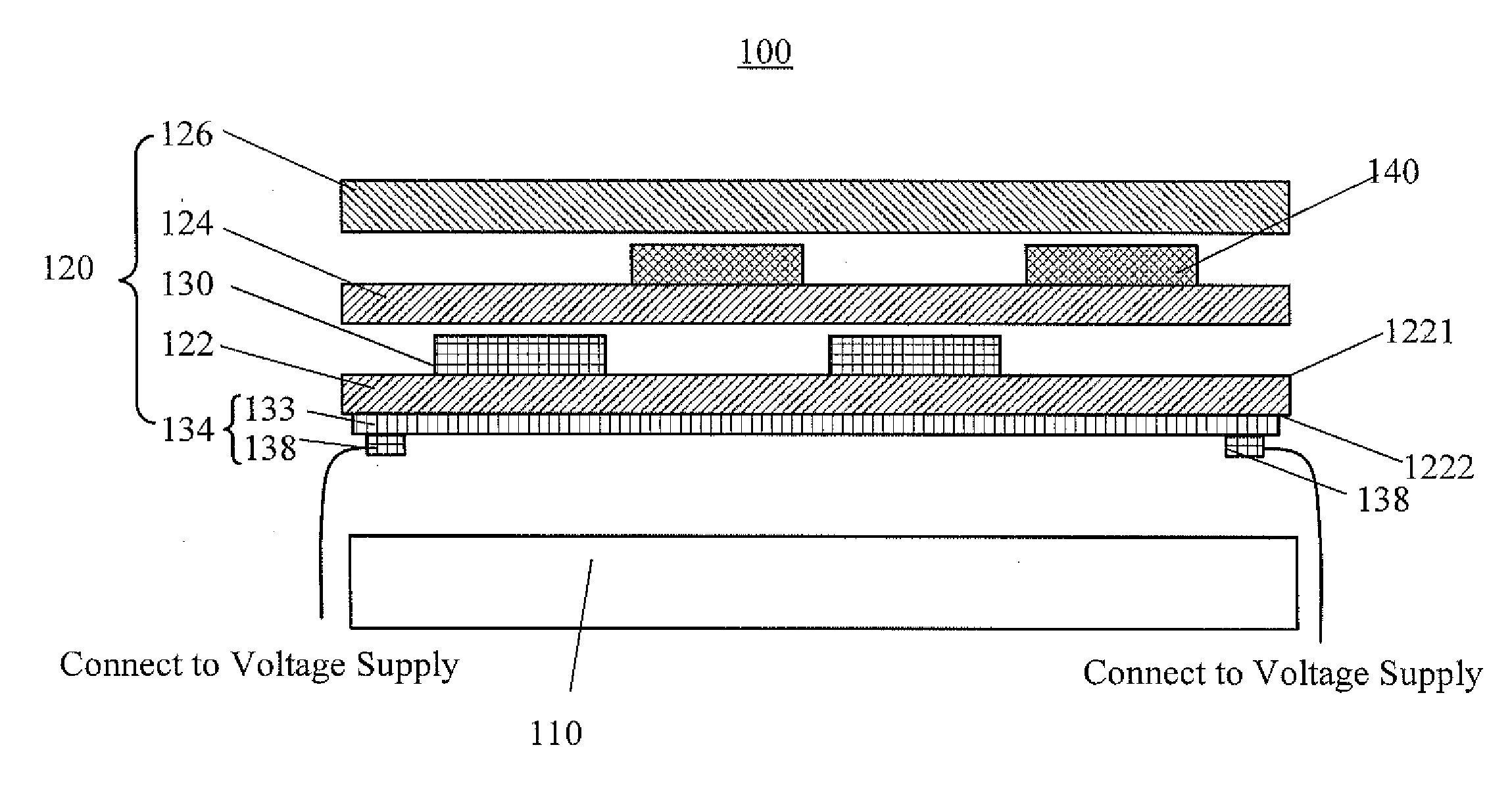
[0032]Referring to FIG. 3 and FIG. 4, FIG. 3 is a structure diagram showing a capacitive touch panel 120 according to the present invention, and FIG. 4 is a cross-sectional view of a display panel 110 comprising the capacitive touch panel 120 in FIG. 3 and a display panel 110. The display panel 110 is, but not limited to, a liquid crystal display (LCD) panel. The display panel 110 comprises upper and lower substrates, a liquid crystal (LC) layer between the upper and lower substrates, and some optical components such as a polarizer film and a color filter. The conducting layer of the upper substrate is electrically connected to common voltage (Vcom). A plurality of pixel electrodes on the lower substrate are charged up to desired data voltage. According to the voltage difference between the data voltage and the common voltage (Vcom), the alignments of the LC molecules of each pixel electrode varies. The optical components and related operating principles used in the LCD panel 110 ar...
third embodiment
[0042]Please refer to FIGS. 10 to 13. FIG. 10 is a top view of a capacitive touch panel 320 according to the present invention. FIG. 11 shows a first conductive circuit 330 and a first shield circuit 350a, a second shield circuit 350b in FIG. 10, FIG. 12 shows a second conductive circuit 340 in FIG. 10, and FIG. 13 is a cross-sectional view of a touch display device comprising the capacitive touch panel in FIG. 10 and a display panel.
[0043]Differing from the touch panel 220 shown in FIGS. 6 to 8, the touch panel 320 comprises the first conductive circuit 330, the first shield circuit 350a, the second shield circuit 350b disposed on the substrate 322, and the second conductive circuit 340 disposed on the substrate 324. In other words, the shield circuit 250 in FIG. 6 is divided into the first shield circuit 350a and the second shield circuit 350b. Both of the first shield circuit 350a and the second shield circuit 350b are symmetrical. The adjacent first shield circuit 350a and secon...
PUM
 Abstract
Description
Claims
Application Information
 - R&D
- Intellectual Property
- Life Sciences
- Materials
- Tech Scout
- Unparalleled Data Quality
- Higher Quality Content
- 60% Fewer Hallucinations
Browse by: Latest US Patents, China's latest patents, Technical Efficacy Thesaurus, Application Domain, Technology Topic, Popular Technical Reports.
© 2025 PatSnap. All rights reserved.Legal|Privacy policy|Modern Slavery Act Transparency Statement|Sitemap|About US| Contact US: help@patsnap.com