
Avalanche photodiode and avalanche photodiode array

a photodiode and array technology, applied in the field of avalanche photodiode and avalanche photodiode array, can solve the problems of light receiving sensitivity, band reduction, and uneven surface amplification factor, and achieve the effect of increasing the aperture ratio

Inactive Publication Date: 2012-11-29
MITSUBISHI ELECTRIC CORP
View PDF6 Cites 7 Cited by
  • Summary
  • Abstract
  • Description
  • Claims
  • Application Information

AI Technical Summary

Benefits of technology

[0010]In view of the above-described problems, an object of the present invention is to provide an avalanche photodiode and an avalanche photodiode array which can realize an increased aperture ratio.
[0012]The present invention makes it possible to realize an increased aperture ratio.

Problems solved by technology

However, the electric field applied to the impurity region is weaker at a distance remote from the electrode, so that the band is reduced.
Also, the amplification factor is not uniform in the surface, and neither is the light receiving sensitivity.
Thus, with the conventional avalanche photodiode, there is a problem that the area of the impurity region cannot be increased above a certain value and, therefore, a high aperture ratio cannot be achieved.
There is also a problem that in a case where a plurality of avalanche photodiodes with electrodes in ring form are arrayed, the aperture ratio is reduced.

Method used


Image

  • Avalanche photodiode and avalanche photodiode array
  • Avalanche photodiode and avalanche photodiode array
  • Avalanche photodiode and avalanche photodiode array

Examples


first embodiment

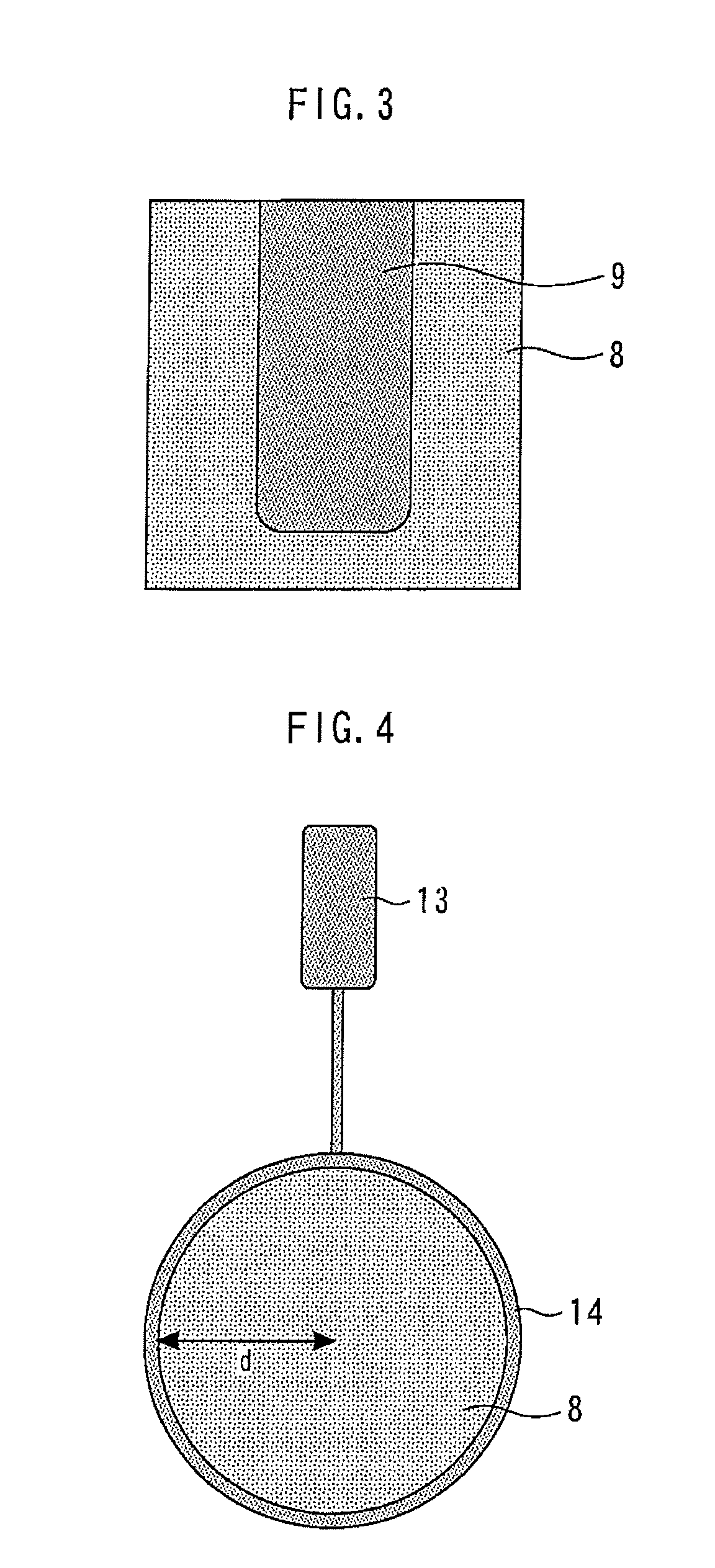
[0034]FIG. 1 is a top view of an avalanche photodiode according to a first embodiment of the present invention. FIG. 2 is a sectional view taken along line I-II in FIG. 1. An n-type InP layer buffer layer 2, an avalanche multiplication layer 3 formed of undoped AlInAs and having a thickness of 0.15 to 0.4 μm, a p-type InP electric field control layer 4 having a thickness of 0.03 to 0.06 μm, a light absorption layer 5 formed of undoped InGaAs and having a thickness of 2 to 3 μm, an undoped InP window layer 6 having a thickness of about 2 μm and an InGaAs contact layer 7 are laid one on another in this order on a major surface of an n-type InP substrate 1. A p-type impurity region 8 is provided in a portion of the undoped InP window layer 6.

[0035]The impurity concentration in the n-type InP substrate is about 5×1018 cm−3; the impurity concentration in the p-type InP electric field control layer 4 is 0.5 to 1×1018 cm−3; and the impurity concentration in the p-type impurity region 8 is ...

second embodiment

[0050]FIG. 7 is a top view of an avalanche photodiode according to a second embodiment of the present invention. The straight A-side electrode 9 has a plurality of straight electrode portions 9a, 9b, and 9c disposed in parallel with each other and an electrode portion 9d perpendicular to a plurality of the electrode portions 9a, 9b, and 9c and connected in common to these electrode portions.

[0051]The distance a is 20 μm. The distance e between each of adjacent pairs of electrode portions 9a and 9b, and 9b and 9c is 40 μm. The width w of each of the electrode portions 9a, 9b, and 9c is 5 μm. The p-type impurity region 8 has a rectangular or corner-rounded rectangular shape as viewed in plan. The length b of the p-type impurity region 8 is longer than the width f.

[0052]The effects of the second embodiment will be described. In the first embodiment, there is a limit to the width c of the p-type impurity region 8 because of use of the single straight p-side electrode 9 (the maximum of w...

third embodiment

[0055]FIG. 8 is a top view of an avalanche photodiode according to a third embodiment of the present invention. The p-type impurity region 8 has a rectangular region 8a in rectangular form as viewed in plan and two semicircular regions 8b respectively joined to shorter sides of the rectangular regions 8a. The semicircular regions 8b are thus joined to the rectangular region 8a to form the p-type impurity region 8 with no angular portions, thereby avoiding electric field concentration such as that at angular corners of the p-type impurity region 8.


PUM


Abstract

An avalanche photodiode including a semiconductor substrate of a first conductivity type, an avalanche multiplication layer, an electric field control layer, a light absorption layer, and a window layer wherein the layers are laid one on another in this order on a major surface of the semiconductor substrate, an impurity region of a second conductivity type in a portion of the window layer, and a straight electrode on the impurity region and connected to the impurity region, the straight electrode being straight as viewed in a plan view facing the major surface of the semiconductor substrate.

Description

BACKGROUND OF THE INVENTION[0001]1. Field of the Invention[0002]The present invention relates to an avalanche photodiode and an avalanche photodiode array which can realize an increased aperture ratio.[0003]2. Background Art[0004]Semiconductor light receiving devices include an avalanche photodiode having a light absorption layer and an avalanche multiplication layer. In an avalanche photodiode disclosed in Japanese Patent Laid-Open No. 62-033482, an electrode and a multiplication layer are adjacent to each other and, therefore, a high electric field can be easily applied to the multiplication layer. A recessed portion is therefore formed in the multiplication layer to suppress edge breakdown. Due to the formation of the recessed portion, however, the process is complicated and the device characteristics vary. On the other hand, an avalanche photodiode disclosed in Japanese Patent Laid-Open No. 2010-135360 has a structure in which an electrode and a multiplication layer are not adja...

Claims


Application Information

Patent Timeline
IPC IPC(8): H01L31/107
CPCH01L31/107H01L31/1075
Inventor SASAHATA, YOSHIFUMINAKAJI, MASAHARU
Owner MITSUBISHI ELECTRIC CORP
Learn More