
Display panel and method of manufacturing the same

a technology of display panel and manufacturing method, which is applied in the field of display panel, can solve problems such as reducing display quality, and achieve the effect of improving the reliability of the alignment layer

Active Publication Date: 2012-08-02
SAMSUNG DISPLAY CO LTD
View PDF11 Cites 44 Cited by
  • Summary
  • Abstract
  • Description
  • Claims
  • Application Information

AI Technical Summary

Benefits of technology

[0008]Exemplary embodiments of the invention provide a display panel capable of improving reliability of an alignment layer.
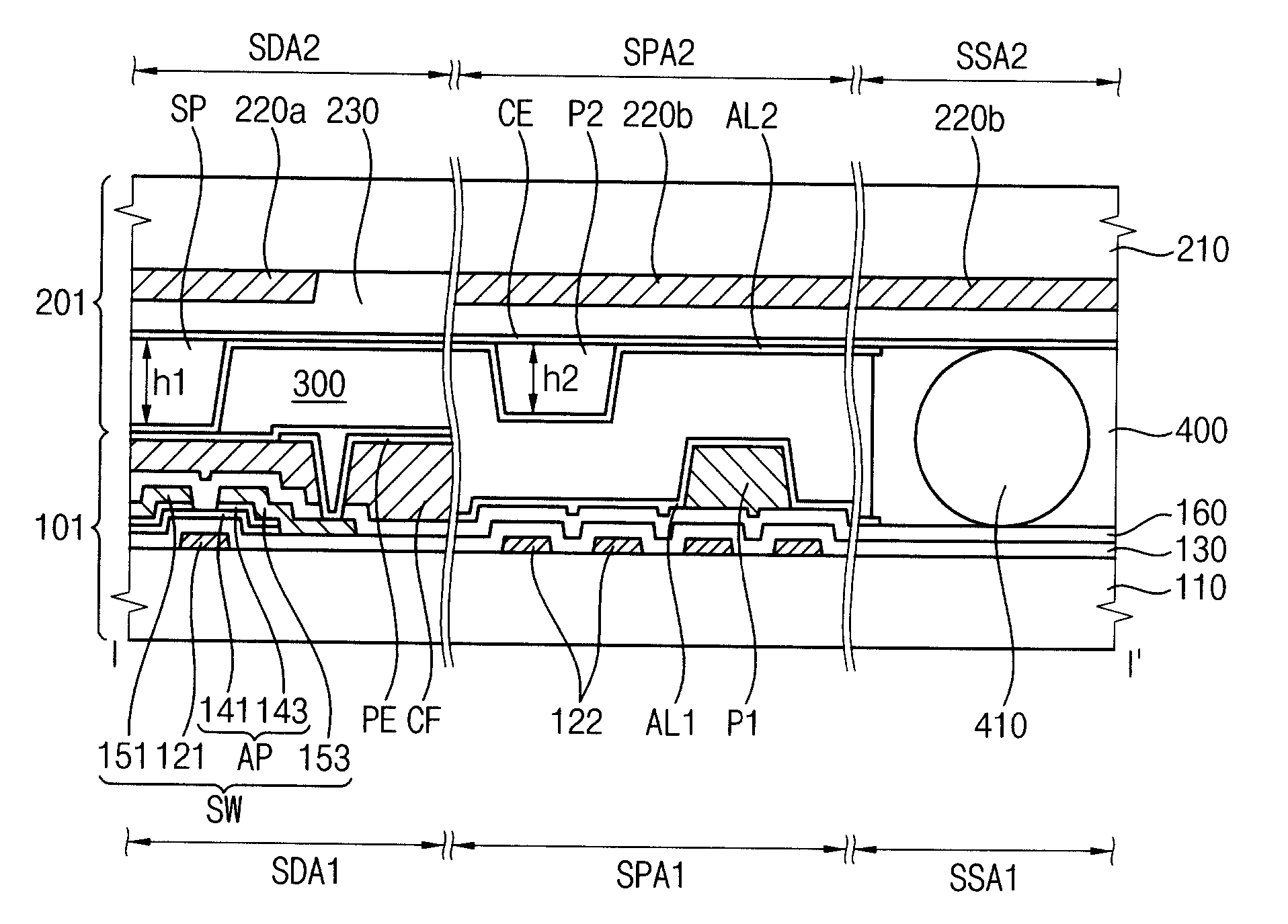
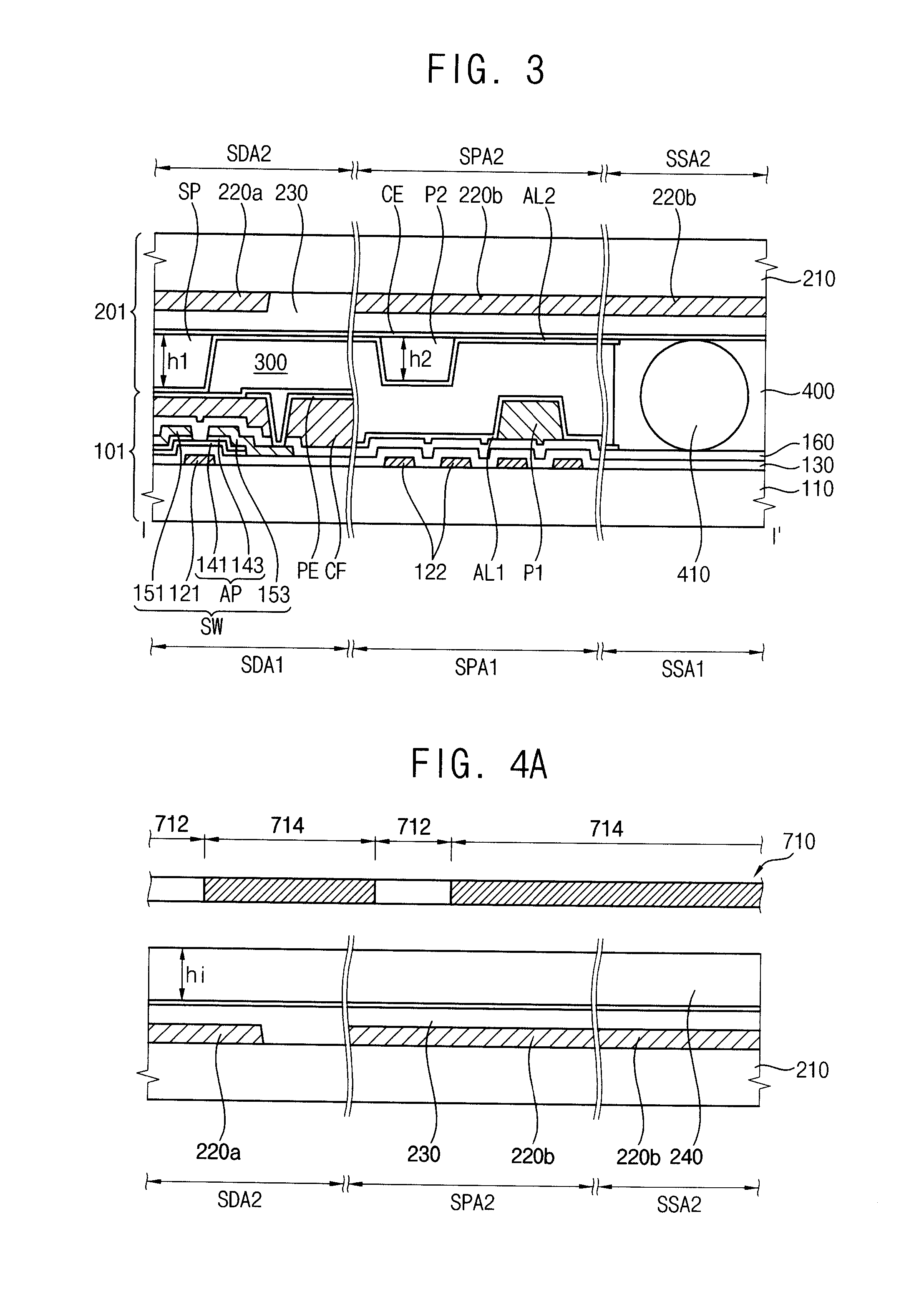
[0012]In an exemplary embodiment, the first display substrate may further include a pixel spacer in the first display region. The pixel spacer may maintain a gap between the first and second display substrates, and be between the first base substrate and the first alignment layer. The first backflow-blocking pattern may be in substantially the same layer as the pixel spacer, and be between the first base substrate and the first alignment layer.
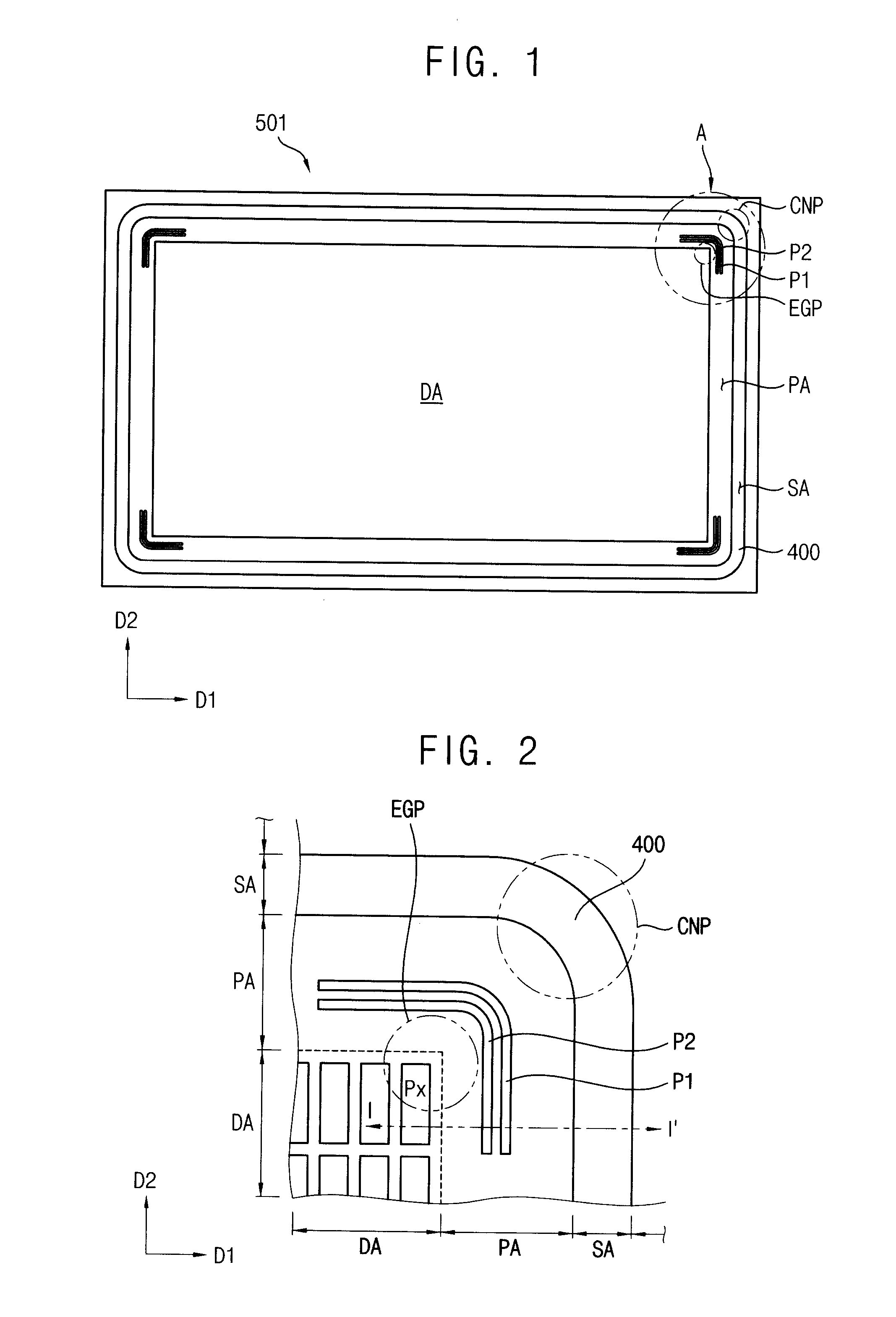
[0022]According to the exemplary embodiments, the backflow-blocking pattern is formed in a peripheral region of at least one of two display substrates of the display panel to reduce or effectively prevent an end portion of the alignment layer, particularly in the corner region of the display substrate, from rolling toward the display region during forming of the alignment layer. The backflow-blocking pattern is simultaneously formed in forming a pixel pattern of a pixel in the display region so that the number of manufacturing processes for the display panel may not be increased.
[0023]In addition, the spread-blocking pattern is additionally formed in a seal line region in which a sealing member is formed, so that the spread-blocking pattern may reduce or effectively prevent the alignment layer from spreading to the seal line region. When the alignment layer is formed in the seal line region, the coherence between the two display substrates is decreased because an adhesive strength between the alignment layer and the sealing member is weak. However, the spread-blocking pattern may reduce or effectively prevent the alignment layer from spreading to the seal line region.

Problems solved by technology

The alignment layer is not formed on a region in which the raw material layer is not formed, and thus the liquid crystal molecules may not be controlled in the region to decrease a display quality.

Method used


Image

  • Display panel and method of manufacturing the same
  • Display panel and method of manufacturing the same
  • Display panel and method of manufacturing the same

Examples


Embodiment Construction

[0043]The foregoing is illustrative of the invention and is not to be construed as limiting thereof. Although a few exemplary embodiments of the invention have been described, those skilled in the art will readily appreciate that many modifications are possible in the exemplary embodiments without materially departing from the novel teachings and advantages of the invention. Accordingly, all such modifications are intended to be included within the scope of the invention as defined in the claims.

[0044]It will be understood that when an element or layer is referred to as being “on” or “connected to” another element or layer, the element or layer can be directly on or connected to another element or layer or intervening elements or layers. In contrast, when an element is referred to as being “directly on” or “directly connected to” another element or layer, there are no intervening elements or layers present. As used herein, “connected” includes physically and / or electrically connecte...


PUM

PropertyMeasurementUnit
Distanceaaaaaaaaaa

Abstract

In a display panel and a method of manufacturing the same, the display panel includes a first display substrate, a second display substrate and a sealing member. The first display substrate includes a first alignment layer in a first display region and a first peripheral region of a first base substrate, and a first backflow-blocking pattern in the first peripheral region and having a curvature to surround a vertex portion of the first display region. The second display substrate includes a second alignment layer in a second display region which faces the first display region and a second peripheral region of a second base substrate. The sealing member includes a corner portion having substantially the same curvature as the first backflow-blocking pattern to surround an outline of the first and second peripheral regions.

Description

[0001]This application claims priority to Korean Patent Application No. 2011-0009426, filed on Jan. 13, 2011, and all the benefits accruing therefrom under 35 U.S.C. §119, the contents of which are herein incorporated by reference in their entireties.BACKGROUND OF THE INVENTION[0002]1. Field of the Invention[0003]Exemplary embodiments of the invention relate to a display panel and a method of manufacturing the display panel. More particularly, exemplary embodiments of the invention relate to a display panel used for a liquid crystal display (“LCD”) apparatus and a method of manufacturing the display panel.[0004]2. Description of the Related Art[0005]Generally, an LCD panel includes a first display substrate including a thin-film transistor (“TFT”) for driving a pixel, a second display substrate facing the first display substrate, and a liquid crystal layer interposed between the first and second display substrates. A voltage is applied to the liquid crystal layer to control light tr...

Claims


Application Information

Patent Timeline
IPC IPC(8): G09G3/36G02F1/1337G06F3/038
CPCG02F1/133723G02F2001/13415G02F1/1341G02F1/1339G02F1/13415G02F1/1337G02F2203/09
Inventor JUNG, YOUNG-MINLIM, SANG-YEOULHONG, KWEON-SAMMOON, HONG-JOONJEONG, YOU-HYUNKIM, SANG-HOLEE, HO-JUN
Owner SAMSUNG DISPLAY CO LTD
Learn More