
Electrode array

a technology of electrode arrays and electrode arrays, applied in the direction of printed circuits, printed circuit details, circuit susbtrate materials, etc., can solve the problems of reducing the effective electrical bonding area between the bonded bonding pads respectively disposed on different electronic devices, unpopular size of the entire display, short circuit, etc., to achieve the effect of reducing the total length, increasing the width of the connecting part, and reducing the effect of the effective electrical bonding area of the interface electrod

Inactive Publication Date: 2012-04-26
E INK HLDG INC
View PDF14 Cites 3 Cited by
  • Summary
  • Abstract
  • Description
  • Claims
  • Application Information

AI Technical Summary

Benefits of technology

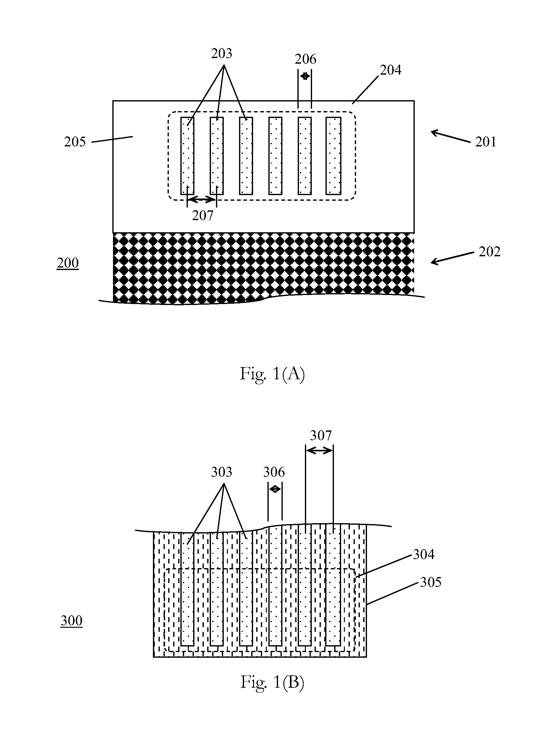
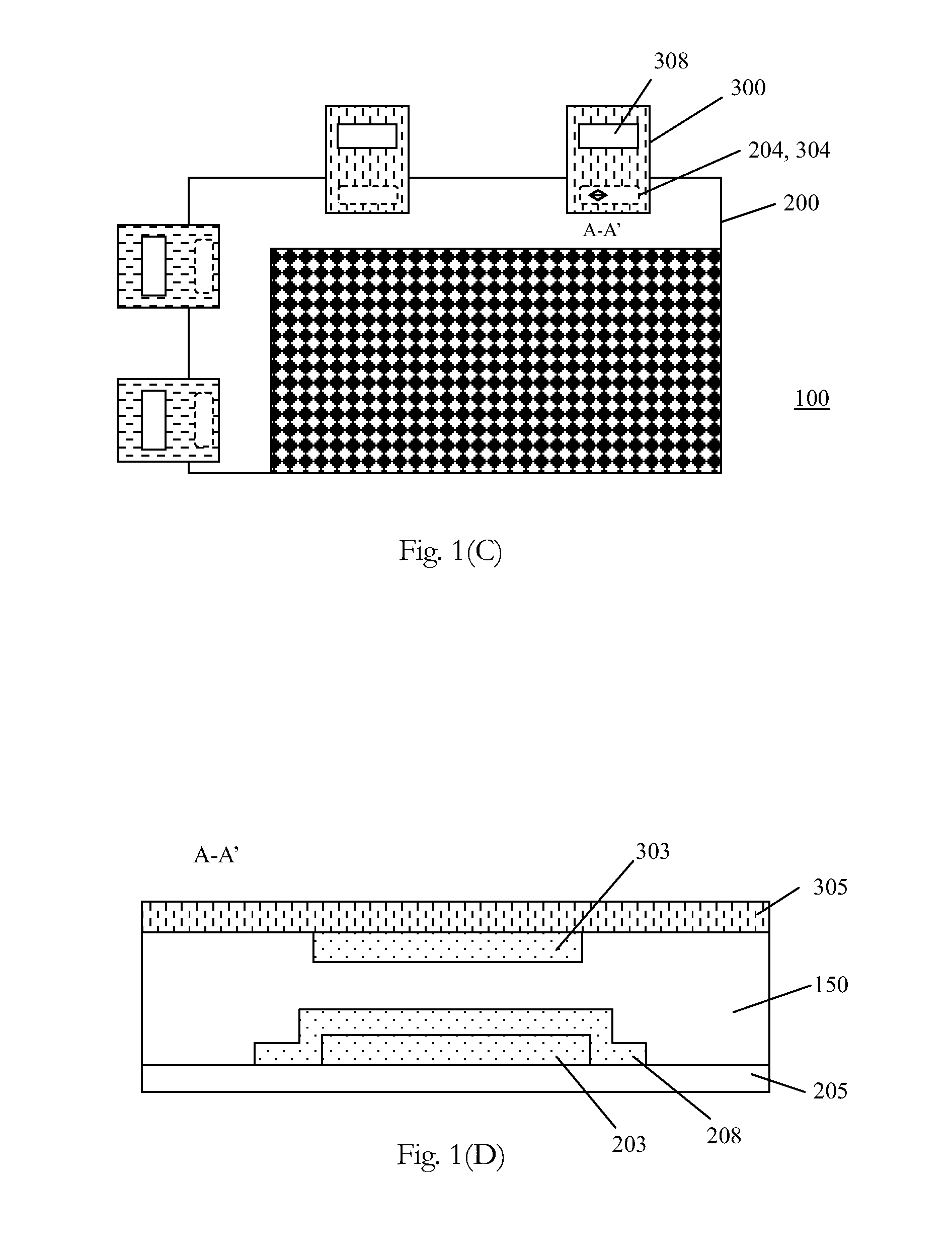
The present invention proposes a method to reduce the size of the interface between electrodes on a display and external circuit, while increasing the width of the interface. This is achieved by arranging multiple connecting parts for each interface electrode in an alternative configuration, resulting in a stagger pattern, a saw-like pattern, or a zigzag pattern. This arrangement effectively enlarges the area for electrically bonding the interface electrodes without changing the pitch or size of the interface region. This reduces the alignment deviation and allows more interface electrodes to be accommodated within a fixed pitch. The invention also provides an electrode array with compensated electrodes that form a stagger, saw-like, or zigzag configuration, and a method for making the electrode array with insulating layers and conductive layers. The technical effects of the invention include reducing the size of the interface between electrodes and improving the alignment accuracy for signal communication between electronic elements.

Problems solved by technology

But the size for entire the display is unpopular to be increased because of consumers' preferences and fashions; on the contrary, the display are manufactured as slimmer and thinner as possible, due to the miniaturization tendency for the electronic device over the consuming market.
However, such development and implementation will cause the effective electrically bonding area between the bonded bonding pads respectively disposed on different electronic device is reduced thereby.
The alignment deviation will result in short circuit.
Furthermore, the alignment deviation will cause the effective electrically bonding area which is originally supposed to be small becomes even much smaller, so that while the bonding pads of the display and the external circuit are electrically connected together by using the ACF, the amounts of the conductive anisotropic particles of the ACF for electrically bridging two bonding pads distributed within the respective effective electrically bonding area will become insufficient, which will result in poor conductive and electronic performance.
However, with the increase of the numbers of the bonding pads and the miniaturization of the dimension itself, the accumulated alignment deviations will exceed the tolerable standard which leads to the failure of the tolerable error.

Method used


Image

  • Electrode array
  • Electrode array
  • Electrode array

Examples


first embodiment

[0037]Please refer to FIG. 2, which is a diagram illustrating the first embodiment according to the present invention. The electrode array in the FIG. 2 disposed within the bonding area 501 of the display 500 includes multiple electrodes 502, each of which have the connecting part 503 and the conductive part 504 wherein a width 505 of the connecting part 503 is larger than a width 506 of the conductive part 504. When the multiple electrodes 502 are arranged, the connecting parts 503 are configured in compensation to each other on the substrate within the bonding area 501, in which the compensation is so presented that the connecting parts 503 preferably appear a configuration in one selected from a group consisting of a stagger pattern, a saw-like pattern and a zigzag pattern. Particularly, the multiple electrodes 502 shown in FIG. 2 are configured in an alternative configuration in density within the bonding area 501.

[0038]While an electrode array consisting of the above-mentioned ...

second embodiment

[0046]In accordance with the above-mentioned principle disclosed, a second embodiment can be correspondingly provided. A display and an external circuit acting as two electronic devices, which are intended in an illustrative rather than in a limiting sense, are embodied as follows.

[0047]With continuous to the first embodiment of FIG. 2, please refer to FIG. 6(A), which is a diagram illustrating a second embodiment according to the present invention. The electrodes 502 of the present invention can be arranged within the bonding area 501 in a sparse arrangement that is not such a dense arrangement as shown in FIG. 2. Thus, the multiple electrodes 502 can be classified into a first class 511 having a first length and a second class 512 having a second length different from the first length. For the condition, the corresponding electrodes within the bonding area of another electronic device can be shaped in a conventional strip.

[0048]It is noted that, when the respective electrodes 502 ...

third embodiment

[0049]A third embodiment is shown in FIG. 6(B). The electrodes 502 in FIG. 6(B) can be classified into a first class 511 having a first length and a second class 512 having a second length different from the first length.

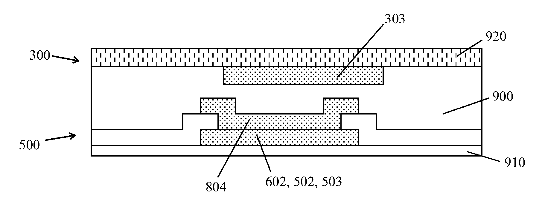
[0050]Please direct to FIG. 7, which is a diagram illustrating the linking state among the bonding pads formed by the electrodes according to the present invention. The bonding area of the display 500 of FIG. 7 has multiple electrodes 602 and 502 manufactured by the method for making an electrode array according to the above-mentioned first to third embodiments. A bonding pad 804 is correspondingly formed above the connecting part 503 of the electrodes 602 and 502. The electrodes 602 and 502 are preferably the electrode with invariable width but variable length or with variable width but invariable length made on the substrate 910 which form an electrode array (only a single electrode but not an electrode array shown in FIG. 7). The bonding area of the external circ...


PUM

PropertyMeasurementUnit
widthaaaaaaaaaa
flexibleaaaaaaaaaa
anisotropic conductiveaaaaaaaaaa

Abstract

An electrode array is provided. The electrode array includes a substrate; and a plurality of electrodes, each of which has a first part with a first width and a second part with a second width different from the first width, wherein the plurality of electrodes are configured in compensation with each other on the substrate.

Description

FIELD OF THE INVENTION[0001]The present invention relates to an electrode array, in particular to an electrode array including multiple electrodes with variable width or length.BACKGROUND OF THE INVENTION[0002]Usually between the display and the external circuit, there is at least one bonding pad used as an interface electrode disposed within the interface region. By electrically linking the bonding pad of the display and that of the external circuit, the display and the external circuit are electrically connected together.[0003]However, with prosperous developments of the electronic technology, the resolution and the responding speed of various displays are continuously enhanced and therefore the signals demanded to be transmitted and received are accordingly increased. But the size for entire the display is unpopular to be increased because of consumers' preferences and fashions; on the contrary, the display are manufactured as slimmer and thinner as possible, due to the miniaturi...

Claims


Application Information

Patent Timeline
Patent Type & Authority Applications(United States)
IPC IPC(8): H05K1/03H05K3/00H05K1/00
CPCH05K1/117H05K1/118Y10T29/49124H05K2201/09709H05K2201/09727H05K3/361
Inventor HUANG, JEN-SHIUNWU, CHI-MINGCHANG, HENG-HAO
Owner E INK HLDG INC
Learn More