Touch panel and method for manufacturing the same
a technology of touch panel and manufacturing method, which is applied in the field of touch panel, can solve the problems of ghost error, interruption of touch, and failure of illustration, and achieve the effect of improving touch sensitivity
- Summary
- Abstract
- Description
- Claims
- Application Information
AI Technical Summary
Benefits of technology
Problems solved by technology
Method used
Image
Examples
first embodiment
[0070 of device
[0071]FIG. 4 is a plan view illustrating a touch panel according to a first embodiment. FIG. 5A is a plan view illustrating a unit cell of FIG. 4 and a region adjacent thereto. FIG. 5B is a plan view illustrating correspondence of a routing line to the unit cell.
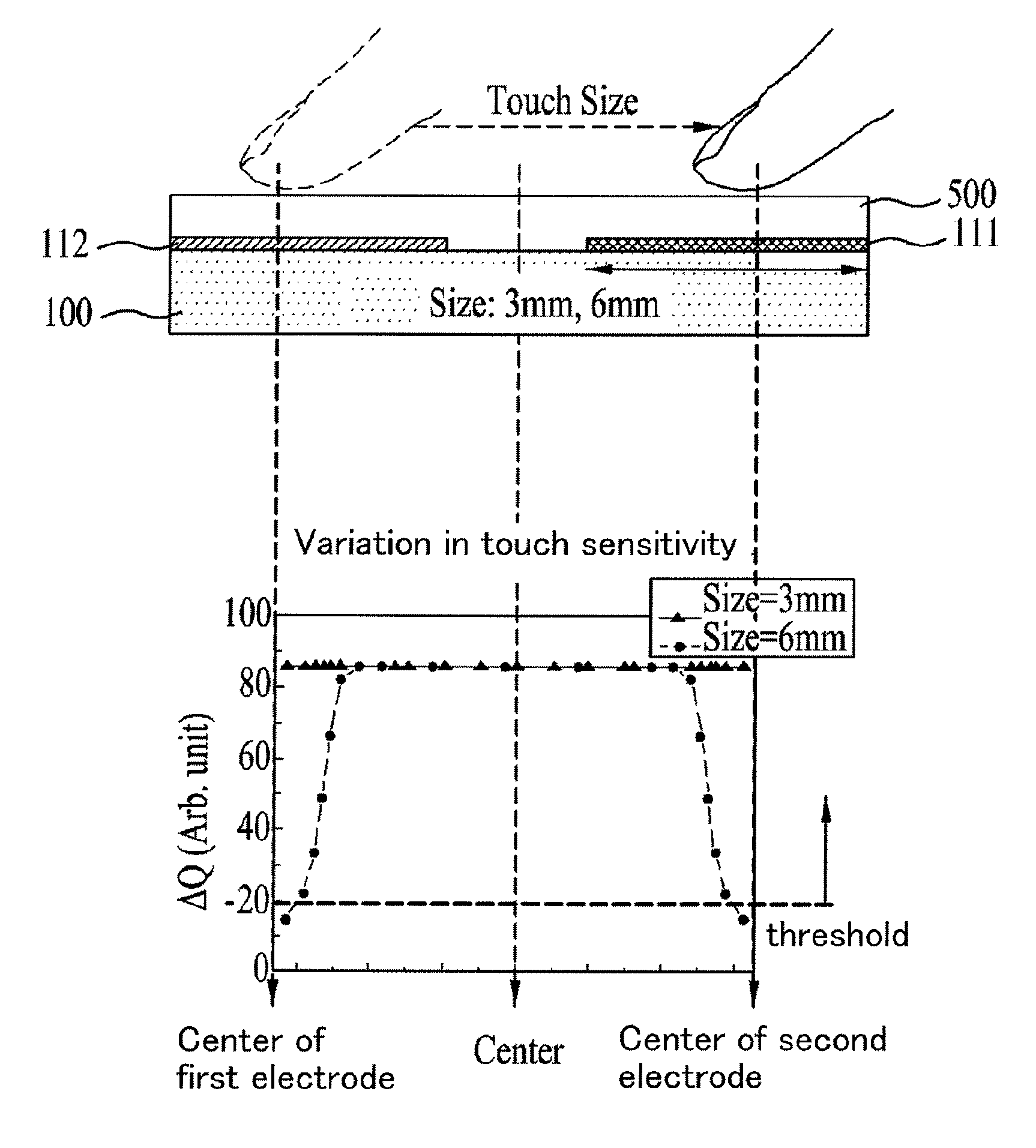
[0072]The touch panel according to the first embodiment, as shown in FIGS. 4 to 5B, includes a plurality of first sensors 1100 arranged in a second direction on the substrate 100, wherein the first sensors (or first electrode serials) 1100 include a plurality of first electrodes (or first electrode patterns) 111 spaced from one another on a substrate 100 in a first direction and a plurality of first bridge patterns (or first connection patterns) 121 to connect the two adjacent first electrodes 111; a plurality of second sensors (or second electrode serials) 1200 arranged in a first direction, wherein the second sensors include a plurality of second electrodes (or second electrode patterns) 112 spaced from one ...
second embodiment
[0113 of device
[0114]FIG. 6 is a plan view illustrating a touch panel according to a second embodiment of the present invention.
[0115]As shown in FIG. 6, the touch panel according to the second embodiment further comprises a dummy pattern 230 between the first electrode 211 and the second electrode 212 adjacent to each other. In this instance, the dummy pattern 230 has a width of about 10 μm to about 240 μm, and the distance between the first electrode 211 and the dummy pattern 230, and the distance between the second electrode 212 and the dummy pattern 230 are about 10 μm to about 30 m.
[0116]The dummy pattern 230 floats and is not connected to a routing line, which is further provided to prevent observation of patterns caused by the location of spaced first and second electrodes 211 and 212 on the intersection between the first and second electrodes 211 and 212. In this instance, the dummy pattern 230 is composed of the same material (i.e., transparent electrode material) as the fi...
third embodiment
[0163 of fabrication method
[0164]FIGS. 12A to 12D are plan views illustrating a method for fabricating a touch panel according to a third embodiment.
[0165]The fabrication method of the touch panel according to the third embodiment is the same as illustrated in FIGS. 10A to 10C of the afore-mentioned first embodiment except that the first and second redundancy patterns 165 and 166 are further patterned with transparent electrodes, as shown in FIG. 12D.
[0166]In this instance, the first redundancy pattern 165 is formed between adjacent first electrodes 161 such that it crosses the first electrodes 161, and the second redundancy pattern 166 is formed between adjacent second electrodes 162 such that it crosses the second electrodes 162.
[0167]Description of the same elements as in first embodiment will be omitted.
PUM
 Abstract
Description
Claims
Application Information
 - R&D
- Intellectual Property
- Life Sciences
- Materials
- Tech Scout
- Unparalleled Data Quality
- Higher Quality Content
- 60% Fewer Hallucinations
Browse by: Latest US Patents, China's latest patents, Technical Efficacy Thesaurus, Application Domain, Technology Topic, Popular Technical Reports.
© 2025 PatSnap. All rights reserved.Legal|Privacy policy|Modern Slavery Act Transparency Statement|Sitemap|About US| Contact US: help@patsnap.com


