Printed circuit board and manufacturing method thereof

a technology of printed circuit boards and manufacturing methods, applied in the direction of printed element electric connection formation, conductive pattern formation, non-metallic protective coating applications, etc., can solve the problems of deteriorating interlayer accuracy, limit to simplification of manufacturing processes,

Inactive Publication Date: 2011-04-21
SAMSUNG ELECTRO MECHANICS CO LTD
View PDF4 Cites 6 Cited by
  • Summary
  • Abstract
  • Description
  • Claims
  • Application Information

AI Technical Summary

Problems solved by technology

However, since the structure is not suitable for high density circuit patterns, a technique of burying circuit patterns in the insulating layer has been introduced.
Here, since a metal barrier is interposed between the carrier and the circuit pattern, there is a limit to simplification of manufacturing processes because the metal barrier has to be etched while the circuit pattern is transferred to the insulating resin.
In that case, an interlayer accuracy may be deteriorated due to the process of opening a portion of the metal barrier.

Method used


Image

  • Printed circuit board and manufacturing method thereof
  • Printed circuit board and manufacturing method thereof
  • Printed circuit board and manufacturing method thereof

Examples


Embodiment Construction

[0015]As the invention allows for various changes and numerous embodiments, particular embodiments will be illustrated in the drawings and described in detail in the written description. However, this is not intended to limit the present invention to particular modes of practice, and it is to be appreciated that all changes, equivalents, and substitutes that do not depart from the spirit and technical scope of the present invention are encompassed in the present invention. In the description of the present invention, certain detailed description of related art is omitted when it is deemed that it may unnecessarily obscure the essence of the invention.

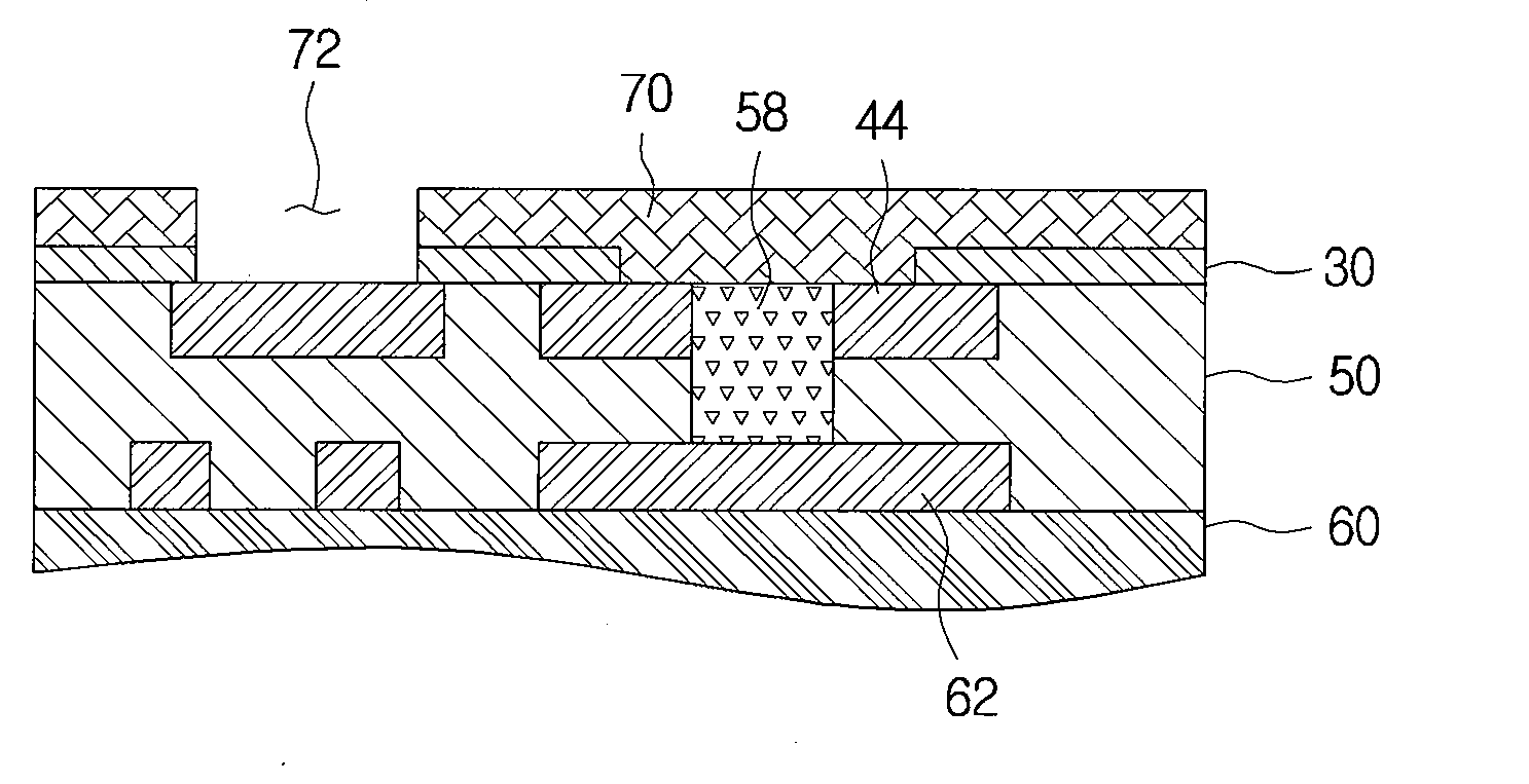
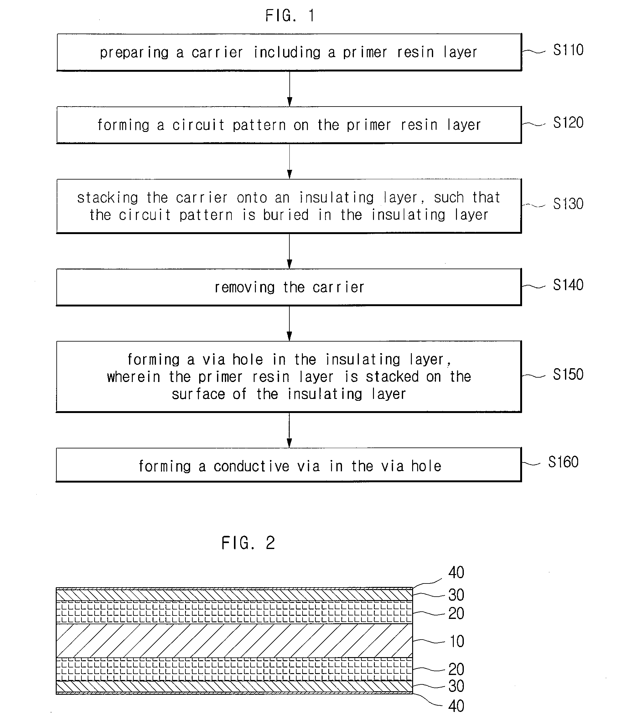
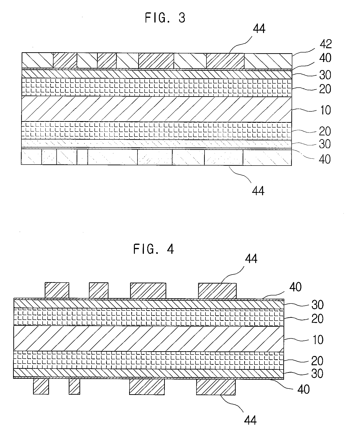
[0016]A printed circuit board and a manufacturing method thereof according to certain embodiments of the present invention will be described below in more detail with reference to the accompanying drawings. Those components that are the same or are in correspondence are rendered the same reference numeral regardless of the figure number...


PUM

PropertyMeasurementUnit
conductiveaaaaaaaaaa
densityaaaaaaaaaa
insulatingaaaaaaaaaa

Abstract

A printed circuit board and a manufacturing method of the same are disclosed. The method includes: preparing a carrier including a primer resin layer formed thereon; forming a circuit pattern on the primer resin layer; stacking the carrier onto an insulating layer such that the circuit pattern is buried in the insulating layer; removing the carrier; forming a via hole in the insulating layer on which the primer resin layer is stacked; and forming a conductive via in the via hole. The conductive via is formed by forming a plating layer in the via hole and on the primer resin layer and removing a portion of the plating layer formed over the primer resin layer.

Description

CROSS-REFERENCE TO RELATED APPLICATIONS[0001]This application claims the benefit of Korean Patent Application No. 10-2009-0099217, filed with the Korean Intellectual Property Office on Oct. 19, 2009, the disclosure of which is incorporated herein by reference in its entirety.BACKGROUND[0002]1. Technical Field The present invention relates to a printed circuit board and a manufacturing method thereof.[0003]2. Description of the Related Art[0004]With the recent trend for a high density multi-functional package board having an electro-device, there has been an increasing demand for high density circuit patterns that are formed on a substrate.[0005]According to the related art, circuit patterns are formed on the surface of an insulating layer. However, since the structure is not suitable for high density circuit patterns, a technique of burying circuit patterns in the insulating layer has been introduced. According to the technique, a carrier is prepared, and a circuit pattern is formed...

Claims


Application Information

Patent Timeline
Patent Type & Authority Applications(United States)
IPC IPC(8): H05K1/02B32B37/00
CPCH05K3/0097H05K3/061H05K3/205H05K3/28H05K3/421H05K3/428H05K3/22H05K2201/09509H05K2201/09563H05K2203/054H05K2203/0571H05K2203/0574H05K3/10H05K3/4658H05K3/20H05K3/40H05K3/18
Inventor LEE, JAE-SEOK
Owner SAMSUNG ELECTRO MECHANICS CO LTD
Why Eureka
Try Eureka