
Capacitive load driving circuit, liquid ejection device, and printing apparatus

Active Publication Date: 2011-01-27
SEIKO EPSON CORP
View PDF1 Cites 18 Cited by
  • Summary
  • Abstract
  • Description
  • Claims
  • Application Information

AI Technical Summary

Benefits of technology

[0007]An advantage of some aspects of the invention is to provide a technique capable of simultaneously realizing the expansion of a voltage range that can be applied to a capacitive load and the improvement of the resolution of voltage change with a small driving circuit.
[0010]According to the capacitive load driving circuit of the aspect of the invention, it is possible to drive the capacitive load with different voltages depending on which charge storage element is selected from the plurality of charge storage elements charged with the different voltages. By changing the charge storage element to be selected, the voltage to be applied to the capacitive load can be changed. When at least two of the charge storage elements are selected, the charge storage elements can be connected to the capacitive load in a state where the charge storage elements are connected in series. Therefore, the voltage to be applied to the capacitive load can be varied depending on a combination of the charge storage elements to be selected. As a result, it is possible to increase the kinds of applicable voltages and expand an applicable voltage range. Nevertheless, since the number of charge storage elements does not have to be increased, a driving circuit of the capacitive load can be miniaturized.
[0012]In the capacitive load driving circuit according to the aspect of the invention, since the plurality of charge storage elements are connected to the capacitive load in the state where the charge storage elements are connected in series, the voltage of the charge storage elements may exceed the voltage of the power supply unit when the plurality of charge storage elements are connected in series. However, by inserting the back-flow preventing unit between the charge storage element and the power supply unit, it is possible to avoid the occurrence of back flow of charge from the charge storage element to the power supply unit.
[0014]In the case where the plurality of voltages generated by the power supply unit satisfy the relation, even when any combination of the voltages is selected, the voltage does not overlap another voltage or a combination of other voltages. Therefore, it is possible to most effectively increase the kinds of applicable voltages and to most effectively expand an applicable voltage range.

Problems solved by technology

In the proposed technique, however, it is difficult to expand an applicable voltage range as well as to improve the resolution of voltage change.
Therefore, it is difficult to change the applied voltage in small steps.
However, this increases the size of a driving circuit because of a great increase in the number of capacitors.

Method used


Image

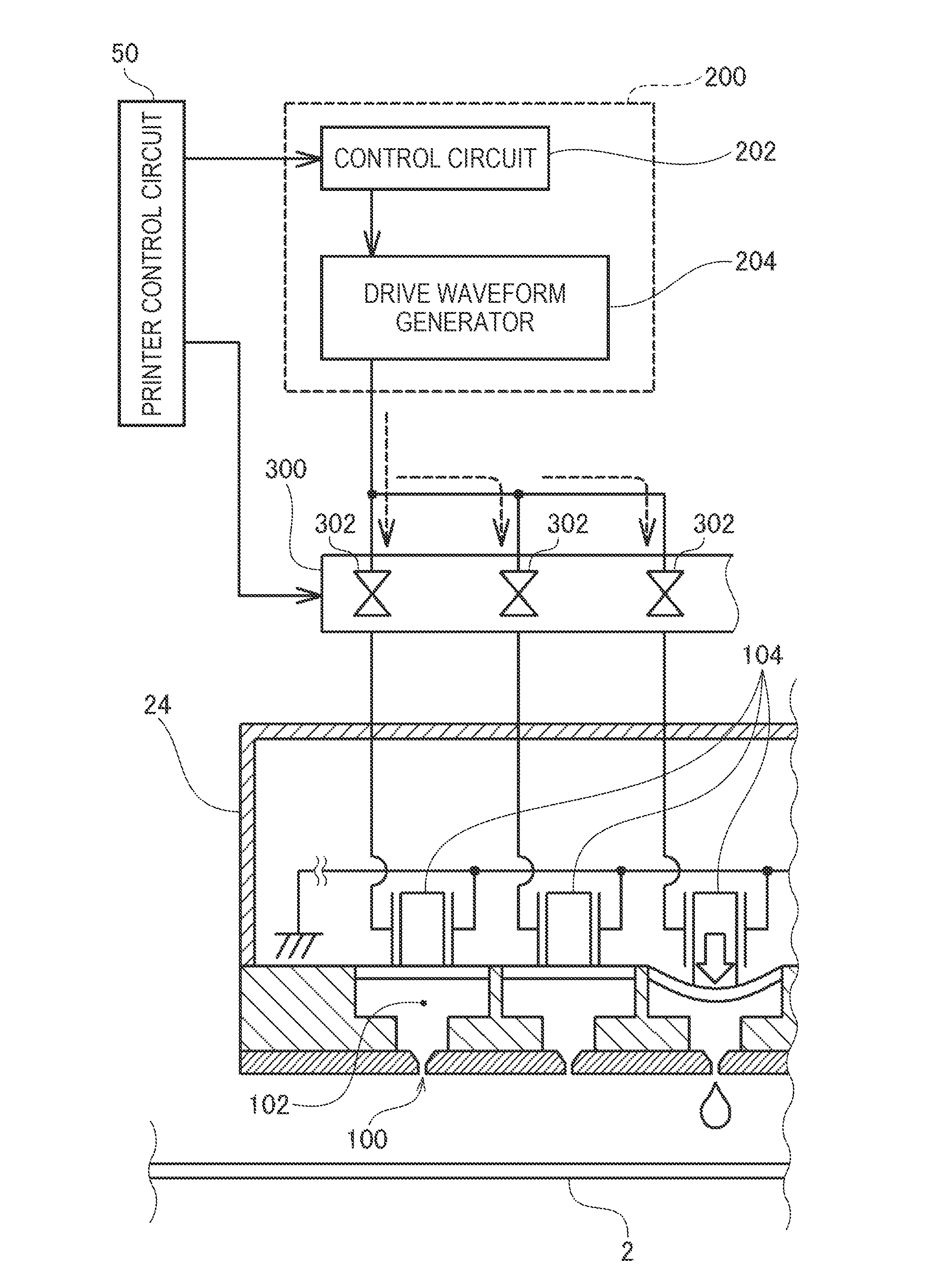
  • Capacitive load driving circuit, liquid ejection device, and printing apparatus
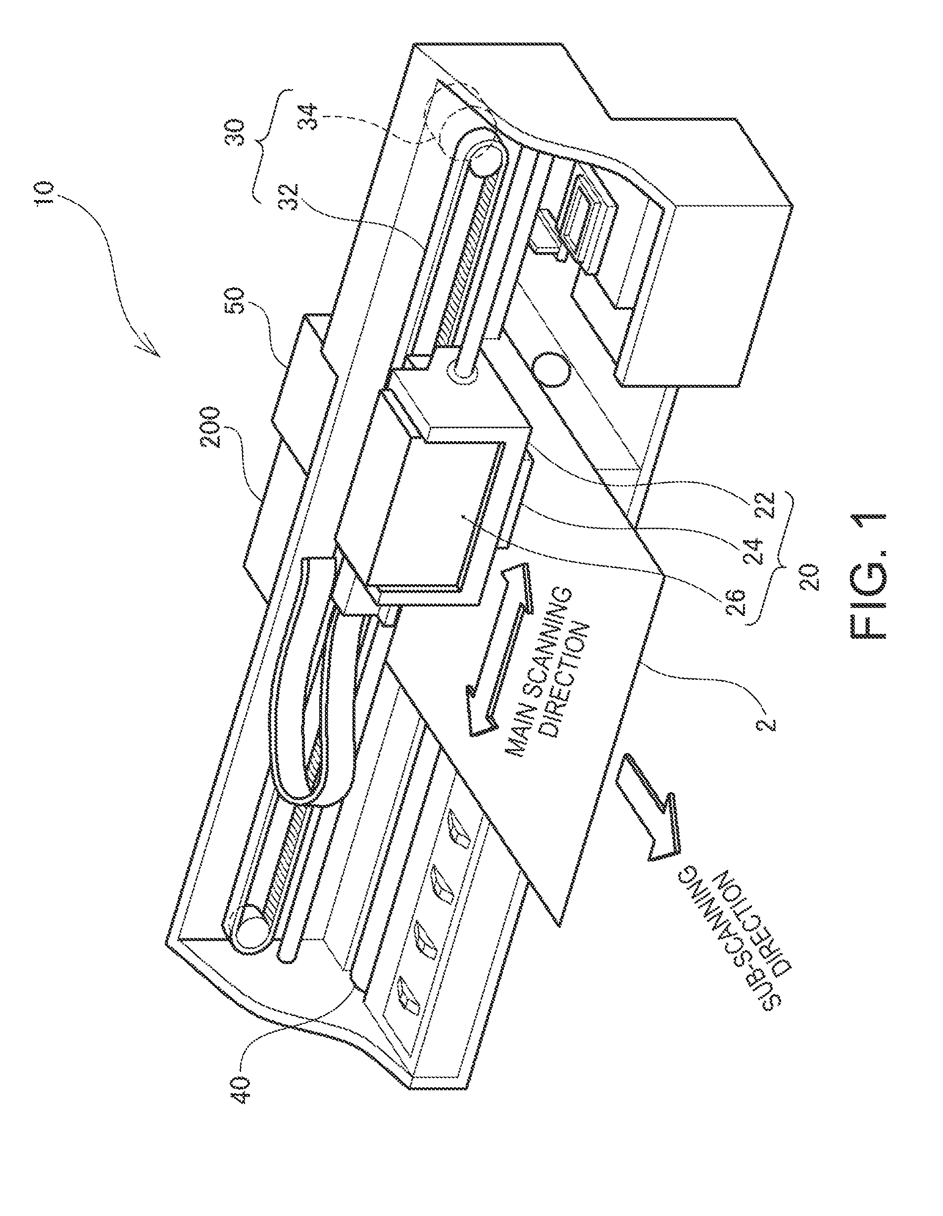
  • Capacitive load driving circuit, liquid ejection device, and printing apparatus
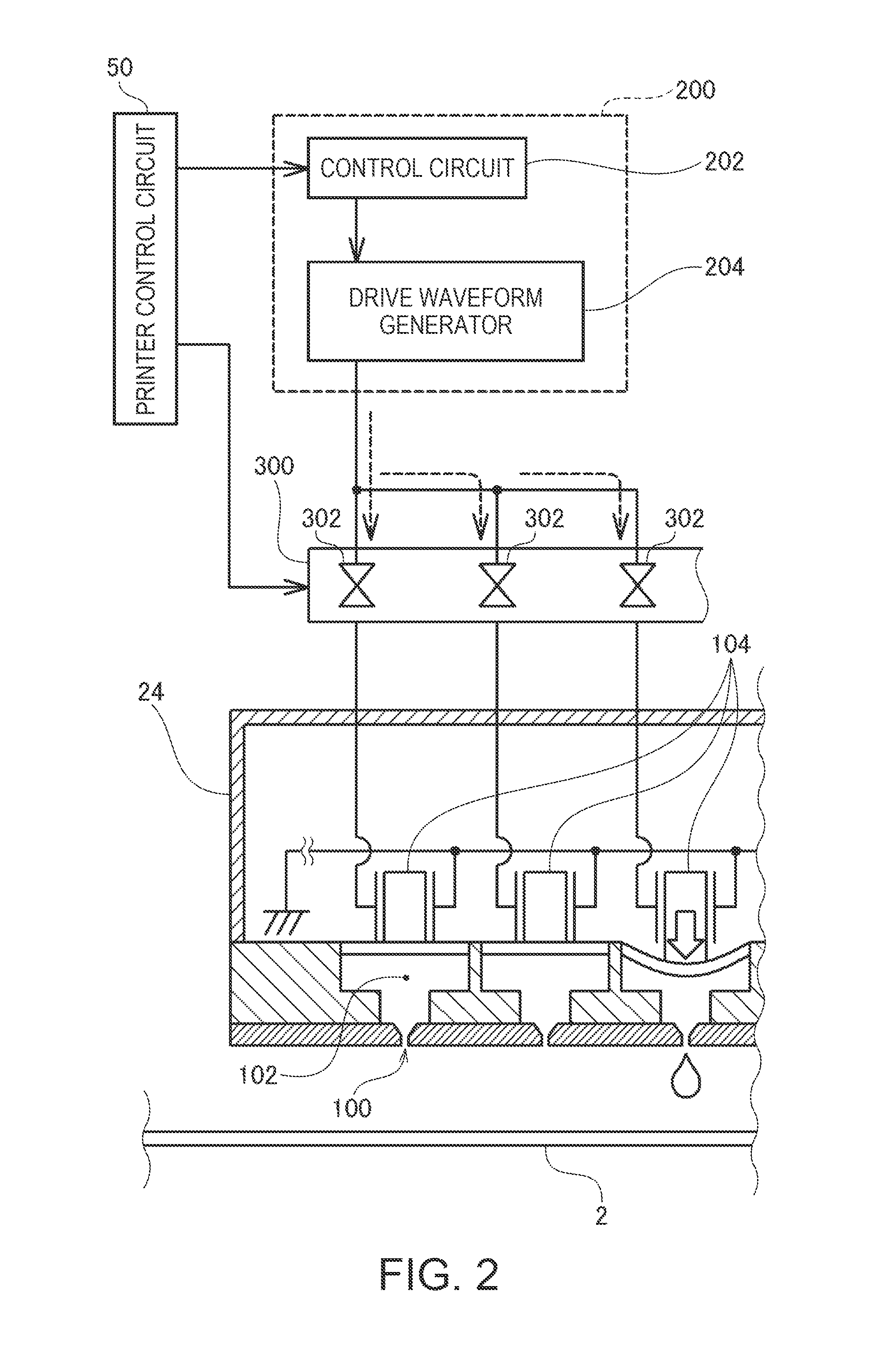
  • Capacitive load driving circuit, liquid ejection device, and printing apparatus

Examples


first modified example

C-1. First Modified Example

[0084]In the drive waveform generator 204 of the above-described embodiment, as switches for switching the connection states of the capacitors C2 to C4, the switches S1 to S4 that can switch between the H state and the L state are used. On the other hand, switches that can switch between the conductive state (ON state) and the disconnected state (OFF state) may be combined for use.

[0085]FIG. 12 is an explanatory view showing the circuit configuration of a drive waveform generator 304 of a first modified example. In the drive waveform generator 304 of the first modified example, the switch S1 is replaced by a switch S1H and a switch S1L compared to the drive waveform generator 204 of the embodiment described with reference to FIG. 3. Similarly, the switch S2 is replaced by a switch S2H and a switch S2L, the switch S3 is replaced by a switch S3H and a switch S3L, and the switch S4 is replaced by a switch S4H and a switch S4L. Also with the drive waveform gen...

second modified example

C-2. Second Modified Example

[0087]In the above-described embodiment, a plurality of power supply circuits that generate different voltages are incorporated in the power supply unit 206. Actually, however, it is sufficient that the power supply unit 206 can generate different voltages. One power supply circuit may generate a plurality of voltages different from one another.

[0088]FIGS. 13A to 13C are explanatory views exemplifying a power supply unit of a second modified example that generates a plurality of voltages from one power supply circuit. For example, like a power supply unit 306 shown in FIG. 13A, a power supply circuit that generates the highest voltage V4 is incorporated, and the voltage generated by the power supply circuit is supplied to step-down DC / DC converters, whereby the plurality of voltages V1 to V3 of different voltages may be generated. Conversely, like a power supply unit 307 shown in FIG. 13B, a power supply circuit that generates the lowest voltage V1 is inc...

third modified example

C-3. Third Modified Example

[0089]In the above-described embodiment and modified examples, the voltages V1 to V4 generated by the power supply units 206 and 306 are fixed. However, the voltages V1 to V4 may be changed according to the driving conditions of the piezo element 104.

[0090]FIG. 14 is a flowchart showing a head driving process of driving the ejection head 24 while changing the voltages V1 to V4 according to the driving conditions of the piezo element 104. The process is executed by a CPU mounted on the printer control circuit 50.

[0091]When the head driving process is started, the CPU of the printer control circuit 50 first determines whether or not it is a drive start timing for the ejection head 24 (step S100). As described above with reference to FIG. 1, since the printer control circuit 50 controls the operation of making the carriage 20 reciprocate, the operation of feeding the print medium, and the operation of the ejection head driving circuit 200 that drives the ejec...


PUM


Abstract

A capacitive load driving circuit that drives a capacitive load, includes: a power supply unit that generates different voltages; a plurality of charge storage elements that are charged with the different voltages generated by the power supply unit; and a load driving section that connects a charge storage element arbitrarily selected from the plurality of charge storage elements to the capacitive load to drive the capacitive load, and connects, when at least two of the charge storage elements are selected, the at least two charge storage elements to the capacitive load in a state where the at least two charge storage elements are connected in series.

Description

CROSS-REFERENCE[0001]This application claims priority to Japanese Patent Application No. 2009-169798, filed on Jul. 21, 2009, the entirety of which is hereby incorporated by reference.BACKGROUND[0002]1. Technical Field[0003]The present invention relates to a technique of driving an electrical load having a capacitive component (capacitive load).[0004]2. Related Art[0005]JP-A-7-130484 discloses a technique in which a plurality of capacitors connected in parallel are previously charged by using a power supply and the capacitors are switched from parallel connection to series connection as needed to generate a voltage higher than a voltage of the power supply, thereby driving an electrical load. By using the proposed technique, it is possible to generate a voltage many times higher than a voltage generated by the power supply according to the number of capacitors connected in series and apply the voltage to the electrical load.[0006]In the proposed technique, however, it is difficult t...

Claims


Application Information

Patent Timeline
IPC IPC(8): B41J29/38H03K3/00
CPCB41J2/04541B41J2/04553H03K4/023B41J2/0457B41J2/04581B41J2/04568
Inventor OSHIMA, ATSUSHITABATA, KUNIOMIYAZAKI, SHINICHIYOSHINO, HIROYUKIIDE, NORITAKA
Owner SEIKO EPSON CORP
Learn More