MEMS Array Substrate and Display Device Using the same
- Summary
- Abstract
- Description
- Claims
- Application Information
AI Technical Summary
Benefits of technology
Problems solved by technology
Method used
Image

Examples
Embodiment Construction
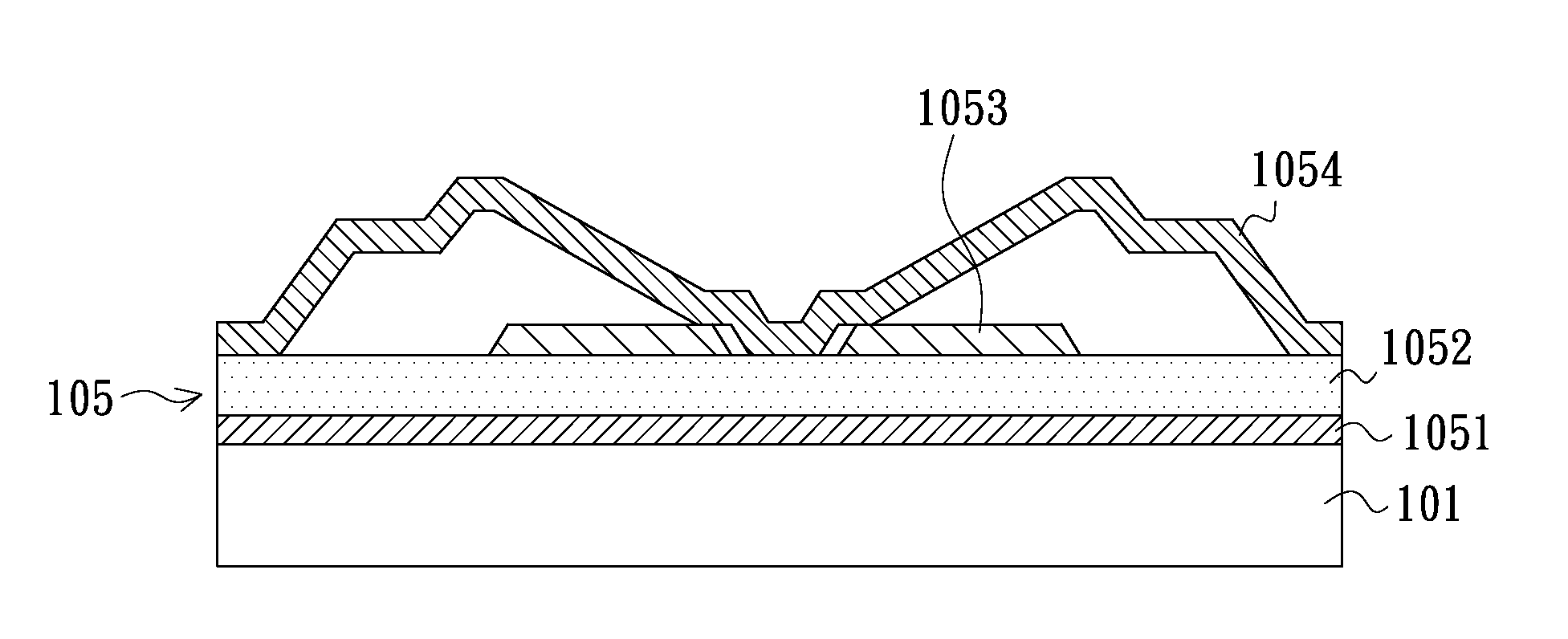
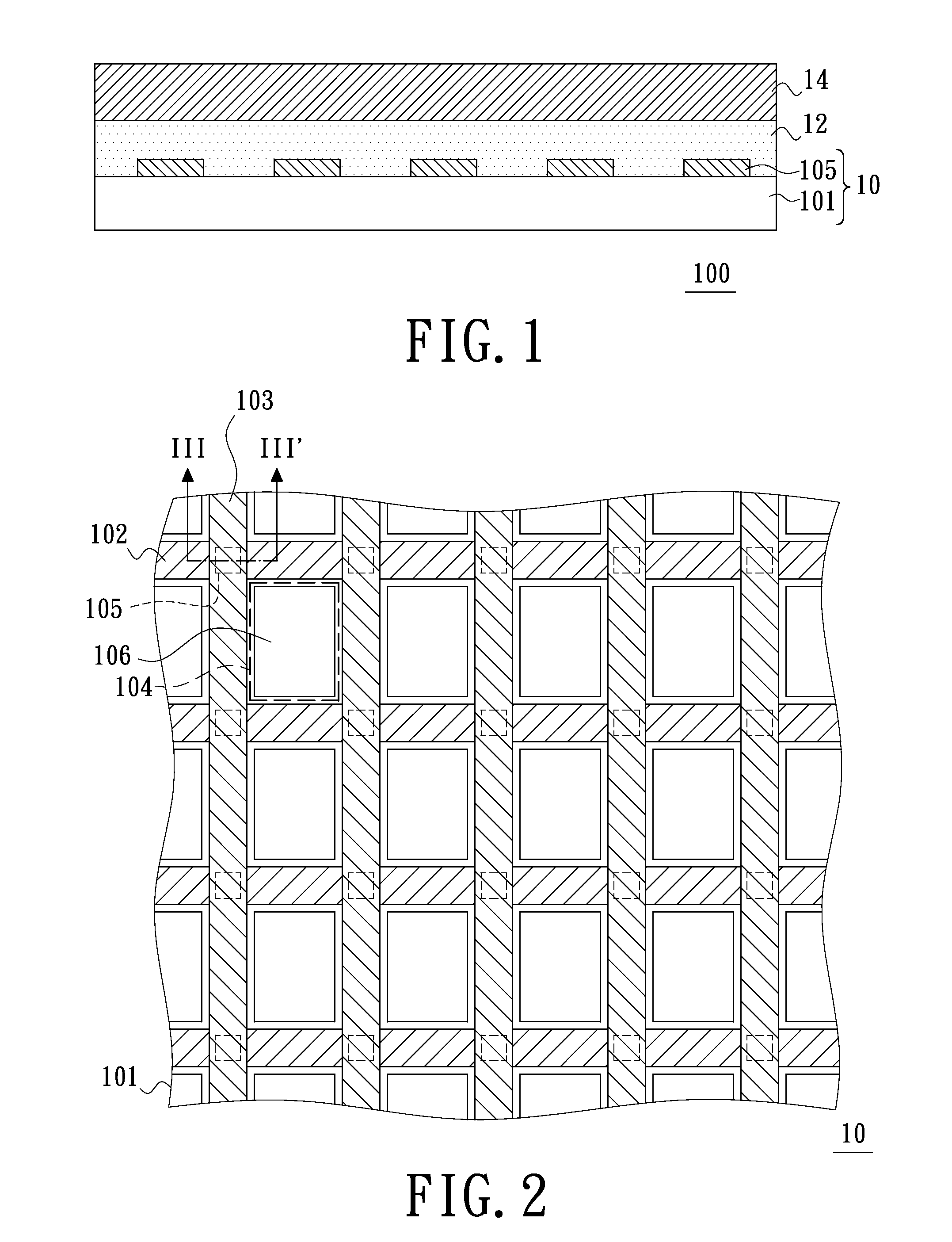
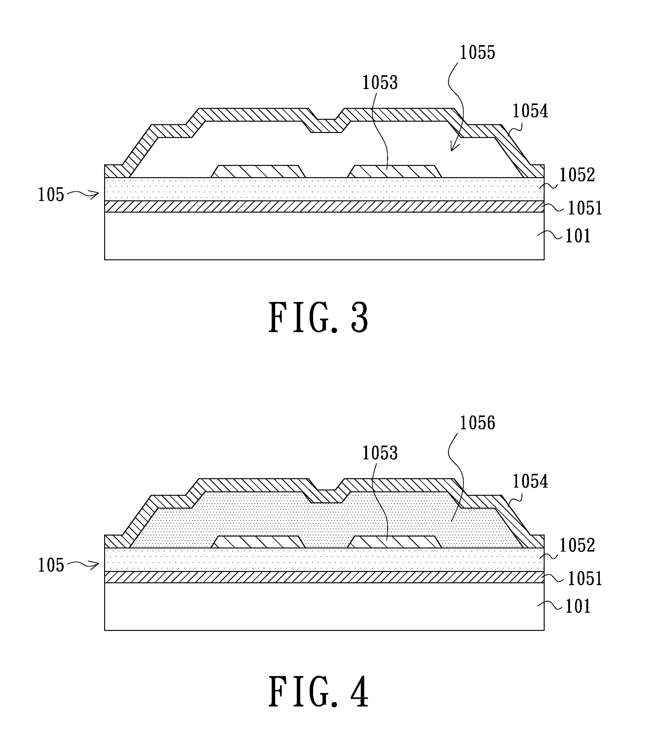
[0021]FIG. 1 is a schematic cross-section view of the display device according to an embodiment of the invention. FIG. 2 is a schematic top view of a MEMS array substrate of the display device shown in FIG. 1. Referring to FIG. 1, the display device 100 includes a MEMS array substrate 10, a display medium layer 12 and a transparent substrate 14. The transparent substrate 14 is disposed above the MEMS array substrate 10, and the display medium layer 12 is disposed between the MEMS array substrate 10 and the transparent substrate 14. Specifically, the display medium layer 12 is, for example, an electro-phoretic layer or a liquid crystal layer.
[0022]Referring to FIG. 1 and FIG. 2, the material of the transparent substrate 14 is, for example, glass. The MEMS array substrate 10 includes a substrate 101, a plurality of first signal lines 102, a plurality of second signal lines 103, a plurality of MEMS switches 105 and a plurality of pixel electrodes 106. The first signal lines 102 are dis...
PUM
 Abstract
Description
Claims
Application Information
 - R&D
- Intellectual Property
- Life Sciences
- Materials
- Tech Scout
- Unparalleled Data Quality
- Higher Quality Content
- 60% Fewer Hallucinations
Browse by: Latest US Patents, China's latest patents, Technical Efficacy Thesaurus, Application Domain, Technology Topic, Popular Technical Reports.
© 2025 PatSnap. All rights reserved.Legal|Privacy policy|Modern Slavery Act Transparency Statement|Sitemap|About US| Contact US: help@patsnap.com