Substrate Processing System and Substrate Processing Device

a processing system and substrate technology, applied in the direction of program control, instruments, total factory control, etc., can solve the problem of the same amount of time and effort, and achieve the effect of increasing the number of connections of process modules

Active Publication Date: 2011-01-06
CANON ANELVA CORP
View PDF2 Cites 4 Cited by
  • Summary
  • Abstract
  • Description
  • Claims
  • Application Information

AI Technical Summary

Benefits of technology

[0008]The present invention has been made in view of above-mentioned problems, and has an object to provide a substrate processing system capable of easily extending and changing the substrate processing module in accordance with changes of processing contents for a substrate.
[0012]According to the present invention, the substrate processing system can be used as one set with the number of connections of process modules increased merely by connecting an additional transfer module to an arbitrary position of the original transfer module without changing the configuration of the transfer module. Therefore, a cost for modifying the transfer module accompanying addition of process modules, etc. can be suppressed, and it is possible to deal with changes promptly.

Problems solved by technology

However, in the case of a device as illustrated in Patent Document 1, it is impossible to connect thereto substrate processing modules in number more than the maximum connection number of the transfer module.In such a case, in order to add substrate processing modules, it is necessary to change the transfer module in such a way as to change a transfer chamber to one having a shape which has more number of connections, and as to increase the number of the transfer chambers to add transfer robots therein.
However, in this case, a program etc. of a transfer control device which controls the transfer robot must be modified as the transfer robot is additionally installed, and in some situation, needed was the same amount of time and effort as to manufacture a new transfer module.

Method used


Image

  • Substrate Processing System and Substrate Processing Device
  • Substrate Processing System and Substrate Processing Device
  • Substrate Processing System and Substrate Processing Device

Examples


Embodiment Construction

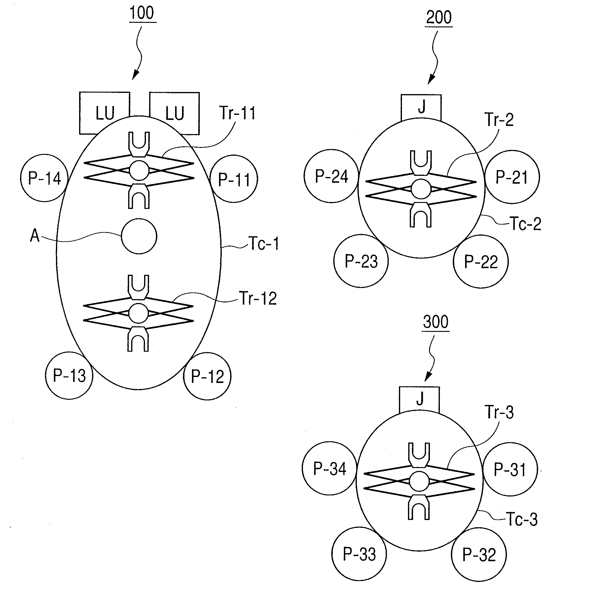
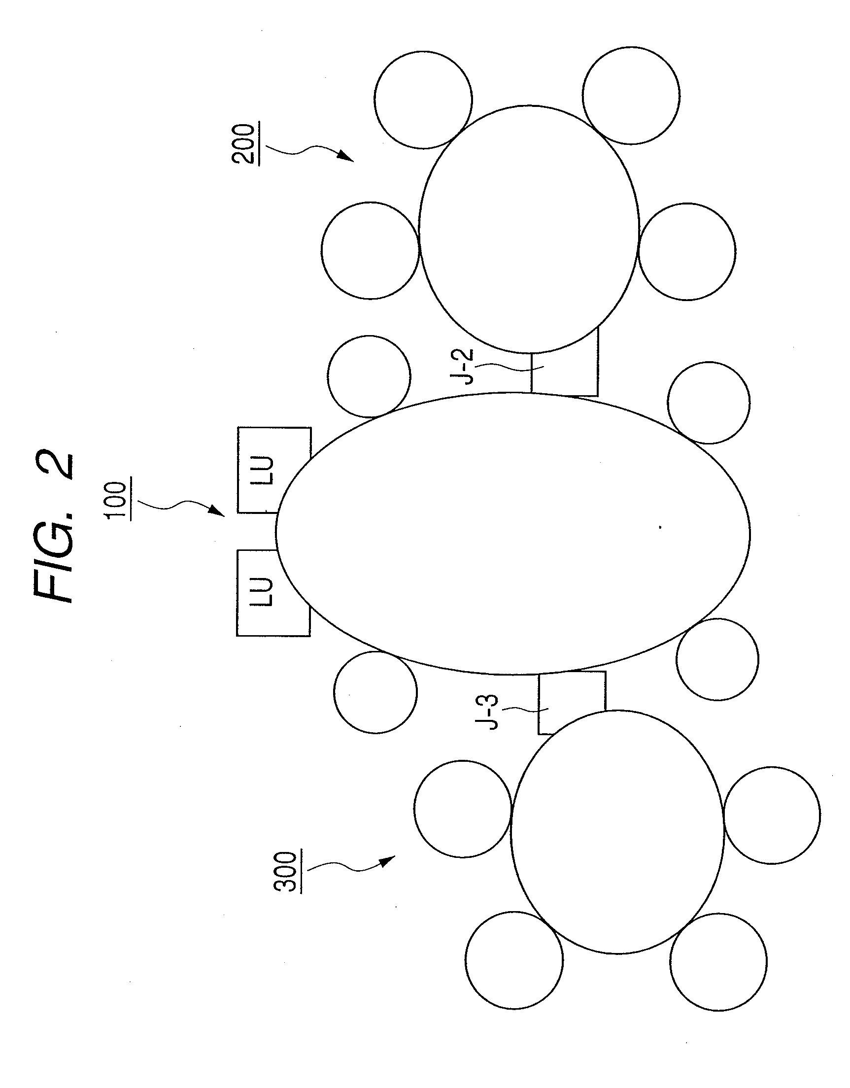
[0026]An embodiment of the present invention will be described with reference to figures.[0027][Regarding a configuration of a substrate processing system and a substrate processing device][0028]FIG. 1 is a figure illustrating a general view of a first substrate processing device 100 (hereinafter called “main device”), a second and a third substrate processing device 200 and 300 (hereinafter called “sub devices”) according to the present embodiment.

[0029]As for the main device 100 of FIG. 1, process chambers P-11 to P-14 are connected via connection ports to a transfer chamber Tc-1 in which transfer robots Tr- and Tr-12 are disposed. Although not illustrated, the transfer chamber Tc-1 of the main device 100 of FIG. 1 has six connection ports, and six process chambers P are connectable thereto. The transfer chamber Tc-1 is connected to a substrate supplying chamber (not shown) via a load-lock / unload-lock chamber LU. A substrate can be introduced in the transfer chamber Tc-1 through t...


PUM

PropertyMeasurementUnit
timeaaaaaaaaaa
stretchableaaaaaaaaaa
displacementaaaaaaaaaa

Abstract

The present invention provides a substrate processing system capable of extending and changing a substrate processing module easily according to changes of processing contents for a substrate. An embodiment of the present invention is the substrate processing system including a main device (100) and sub devices (200 and 300). A transfer controlling part (130) includes: a transfer-procedure acquiring part (131) acquiring transfer-destination specifying information that includes additional information capable of identifying at least a local address and a substrate processing device to which the local address belongs, and that specifies a substrate transfer destination uniquely within the main device (100) and the sub devices (200 and 300); a transfer-destination judging part (132) capable of judging which one of the main device (100), the sub device (200) and the sub device (300) is the substrate transfer destination based on the transfer-destination specifying information acquired by the transfer-procedure acquiring part (131); and a local transfer part (133) that transfers the substrate to a process chamber connected to a transfer chamber of its own device by using the local address allocated uniquely within the own device.

Description

CROSS-REFERENCES TO RELATED APPLICATIONS[0001]This application is a continuation application of International Application No. PCT / JP2009 / 069475, filed on Nov. 17, 2009, the entire contents of which are incorporated by reference herein.[0002]This application also claims the benefit of priority from Japanese Patent Application No. 2008-335778 filed Dec. 29, 2008, the entire contents of which are incorporated herein by reference.TECHNICAL FIELD[0003]The present invention relates to a substrate processing system and substrate processing device capable of easily making additional installation and change in accordance with changes, etc. of processing contents for a substrate.BACKGROUND ART[0004]Conventionally, as a substrate processing device which manufactures electronic parts such as a semiconductor device and a memory element, there is known a cluster type substrate processing device with a plurality of substrate processing modules connected to a transfer module provided with a transfe...

Claims


Application Information

Patent Timeline
Patent Type & Authority Applications(United States)
IPC IPC(8): B65G43/00G06F19/00
CPCG05B19/4189H01L21/67276G05B2219/45031G05B2219/32006Y02P90/02
Inventor KOBAYASHI, HIROHITO
Owner CANON ANELVA CORP
Why Eureka
Try Eureka