Method for verification of mask layout of semiconductor integrated circuit
- Summary
- Abstract
- Description
- Claims
- Application Information
AI Technical Summary
Benefits of technology
Problems solved by technology
Method used
Image
Examples
first embodiment
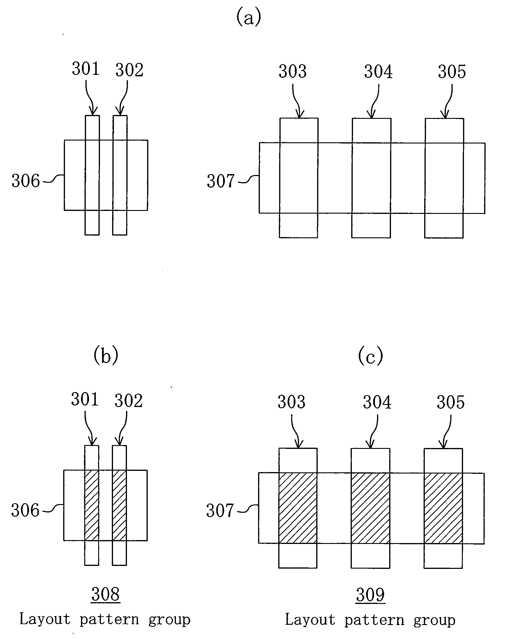
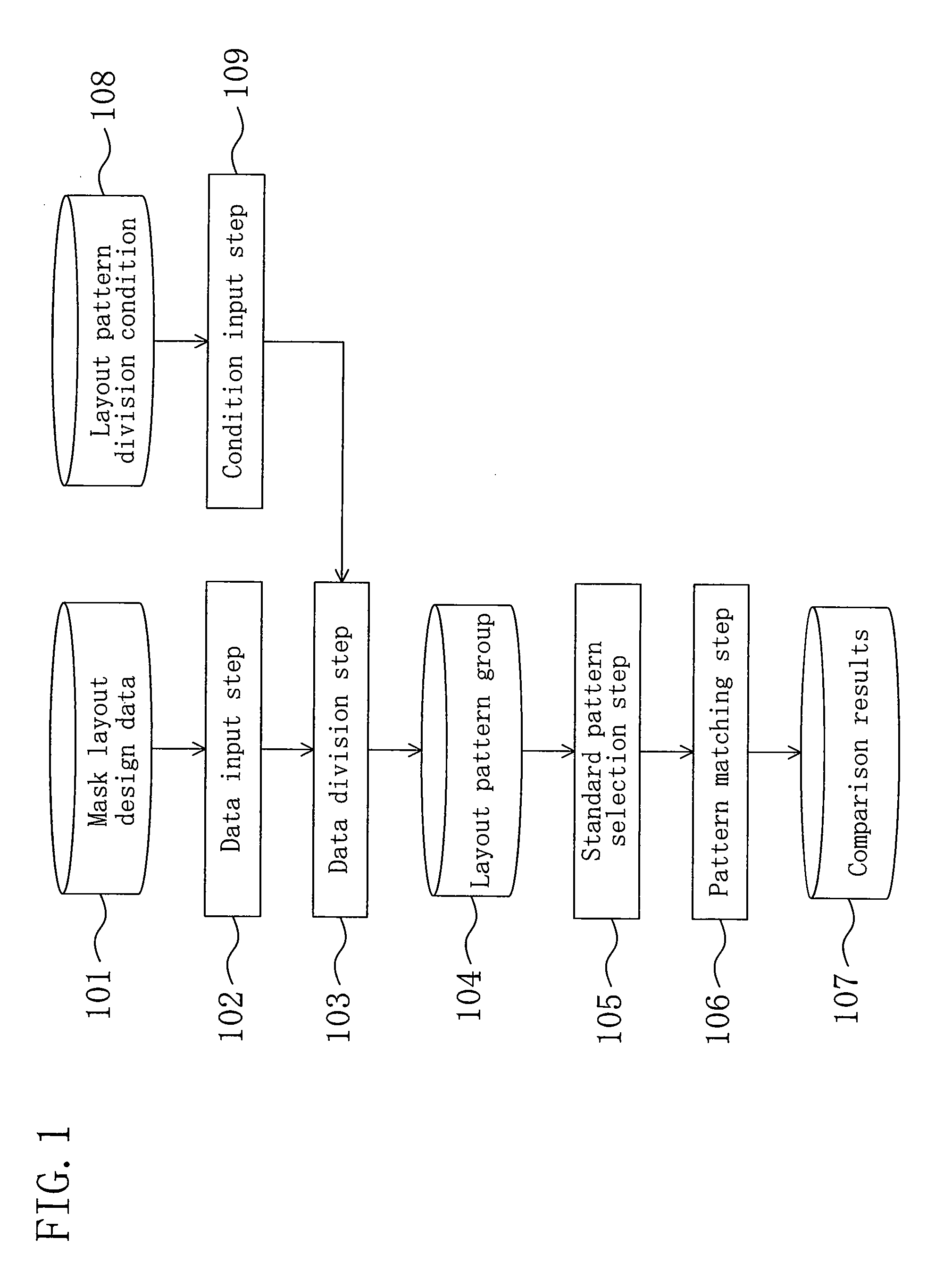
[0052]FIG. 1 is a flowchart of a semiconductor integrated circuit mask layout verification method using a computer according to a first embodiment of the present invention.
[0053]In FIG. 1, mask layout design data 101 is first read in a data input step 102. Next, a layout pattern division condition 108 is read in a condition input step 109.
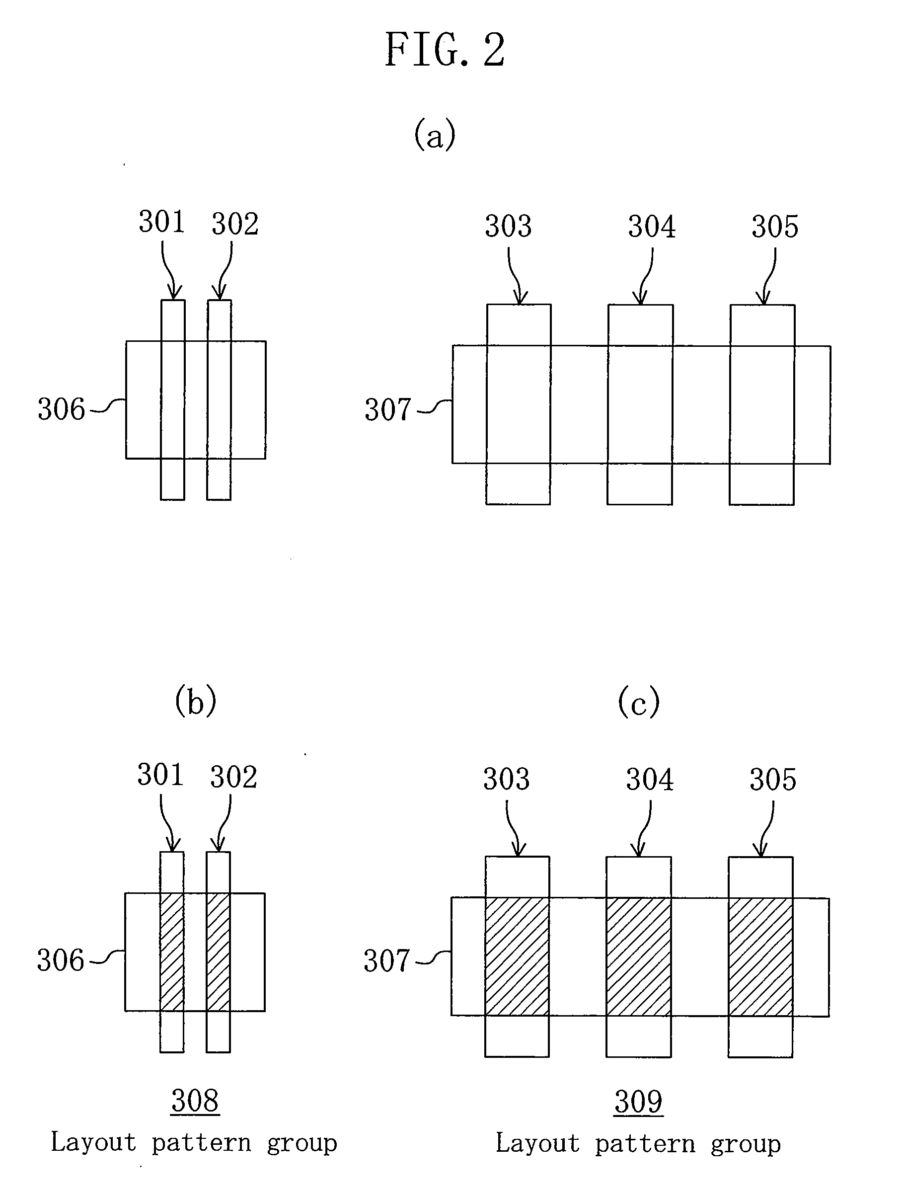
[0054]Then, in a data division step 103, the mask layout design data 101 read in the data input step 102 is divided into layout pattern groups according to the layout pattern division condition 108 read in the condition input step 109, and the layout pattern groups 104 are output.
[0055]Subsequently, in a standard pattern selection step 105, a standard pattern is individually selected from each of the divided layout pattern groups 104 as a standard used in pattern matching performed for layout patterns included in that layout pattern group 104.
[0056]Then, in a pattern matching step 106, comparisons (e.g., pattern matching) are made between the layou...
second embodiment
[0062]Next, a second embodiment of the present invention will be described.
[0063]In the first embodiment, in the data division step 103, data division depending on mask shapes has been described by way of example. In this embodiment, mask layout design data is divided according to circuit connection information.
[0064]FIG. 5 shows mask layout design data according to this embodiment. In this design data, layout patterns 210, 212, and 214 of three transistors connected to a signal wiring 207, and layout patterns 211 and 213 of two transistors connected to a signal wiring 208 are present.
[0065]In this embodiment, the layout pattern division condition 108 in the condition input step 109 is circuit connection information. For example, in the mask layout design data of FIG. 5, the signal wiring 207 or 208 is specified as the circuit connection information.
[0066]When the layout pattern division condition 108 in the condition input step 109 is the signal wiring 207, the layout pattern group...
third embodiment
[0069]Next, a third embodiment of the present invention will be described.
[0070]In the first embodiment, a layout pattern closest to the origin point (0, 0) of the coordinate system of each of the divided layout pattern groups is selected as a standard pattern in the standard pattern selection step 105. In this embodiment, regions 405 and 406 that include layout patterns located around standard patterns 401 and 402 are entirely selected as standard patterns as shown in FIGS. 8(a) and 8(b).
[0071]In FIGS. 8(a) and 8(b), when compared with each other, the layout patterns 401 and 402 of two transistors have the same shape, however, the regions 405 and 406 that include the areas surrounding these layout patterns 401 and 402 have different shapes. In a case in which the layout patterns 401 and 402 are composed of transistors (semiconductor devices), the device characteristics may vary depending not only on the shapes of the semiconductor devices, but also on the effects of the layout patt...
PUM
 Abstract
Description
Claims
Application Information
 - R&D
- Intellectual Property
- Life Sciences
- Materials
- Tech Scout
- Unparalleled Data Quality
- Higher Quality Content
- 60% Fewer Hallucinations
Browse by: Latest US Patents, China's latest patents, Technical Efficacy Thesaurus, Application Domain, Technology Topic, Popular Technical Reports.
© 2025 PatSnap. All rights reserved.Legal|Privacy policy|Modern Slavery Act Transparency Statement|Sitemap|About US| Contact US: help@patsnap.com


