
Spare cell library design for integrated circuit

a technology of integrated circuits and libraries, applied in the field of separate cell library design for integrated circuits, can solve problems such as leakage through vdd, vss and the gate, and is not used to realize intended logic or work, and achieves the effect of reducing the amount of dispersed leakage power, and reducing the number of used

Inactive Publication Date: 2010-09-16
FREESCALE SEMICON INC
View PDF3 Cites 13 Cited by
  • Summary
  • Abstract
  • Description
  • Claims
  • Application Information

AI Technical Summary

Problems solved by technology

The unselected spare cells are typically added to the ASIC design but are not used to realize the intended logic or working functionality of the ASIC.
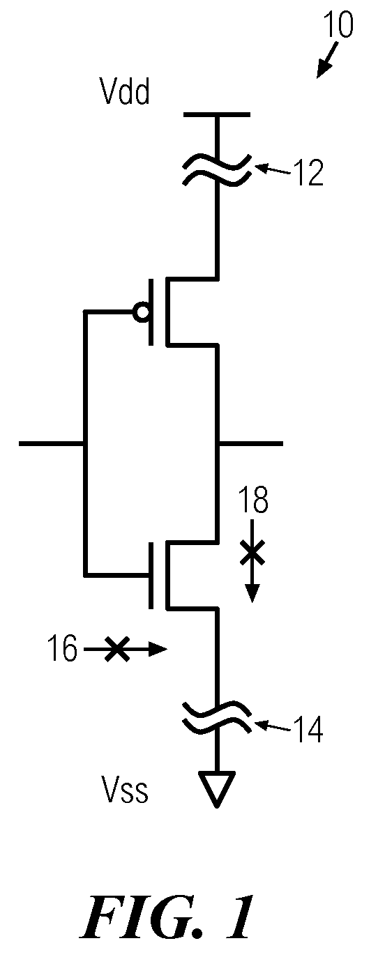
This results in leakage through Vdd, Vss and the gate and adds to dissipated leakage power.
With the ever increasing emphasis on reducing power, conventional cell libraries are power intensive.
Additionally, the limitations of conventional standard cell libraries include the constant leakage current paths.
This leakage of functionally unused spare cells that remain connected to the power source increases in magnitude as the demand for the number of spare cells increases, which results in overhead on the cell design and reduces the choice of cell sets for spare modules.
This also reduces the spare cell density in the design.
In traditional ASIC cell based designs, it is proving more difficult to implement ECO and close timing of timing critical paths.
The conventional standard spare cells used for repair constantly consume leakage current.
The spare cells in traditional standard cell libraries continue to consume leakage current even if the spare cells are not used functionally.
This all contributes to increasing power consumption in the conventional spare cell library designs.
However, with the ever increasing density of cells, has come the even more dramatic increase in the overall power consumption.
Each cell whether a functional logic base cell or spare cell contributes to the overall power consumption of the ASIC.
Every spare cell, even the spare cells that remain unconnected to the functional logic base cell and do not become part of the working functionality of the ASIC, are connected to ground and power before and after the metallization process which contribute to the overall power consumption of the ASIC.

Method used


Image

  • Spare cell library design for integrated circuit
  • Spare cell library design for integrated circuit
  • Spare cell library design for integrated circuit

Examples


Embodiment Construction

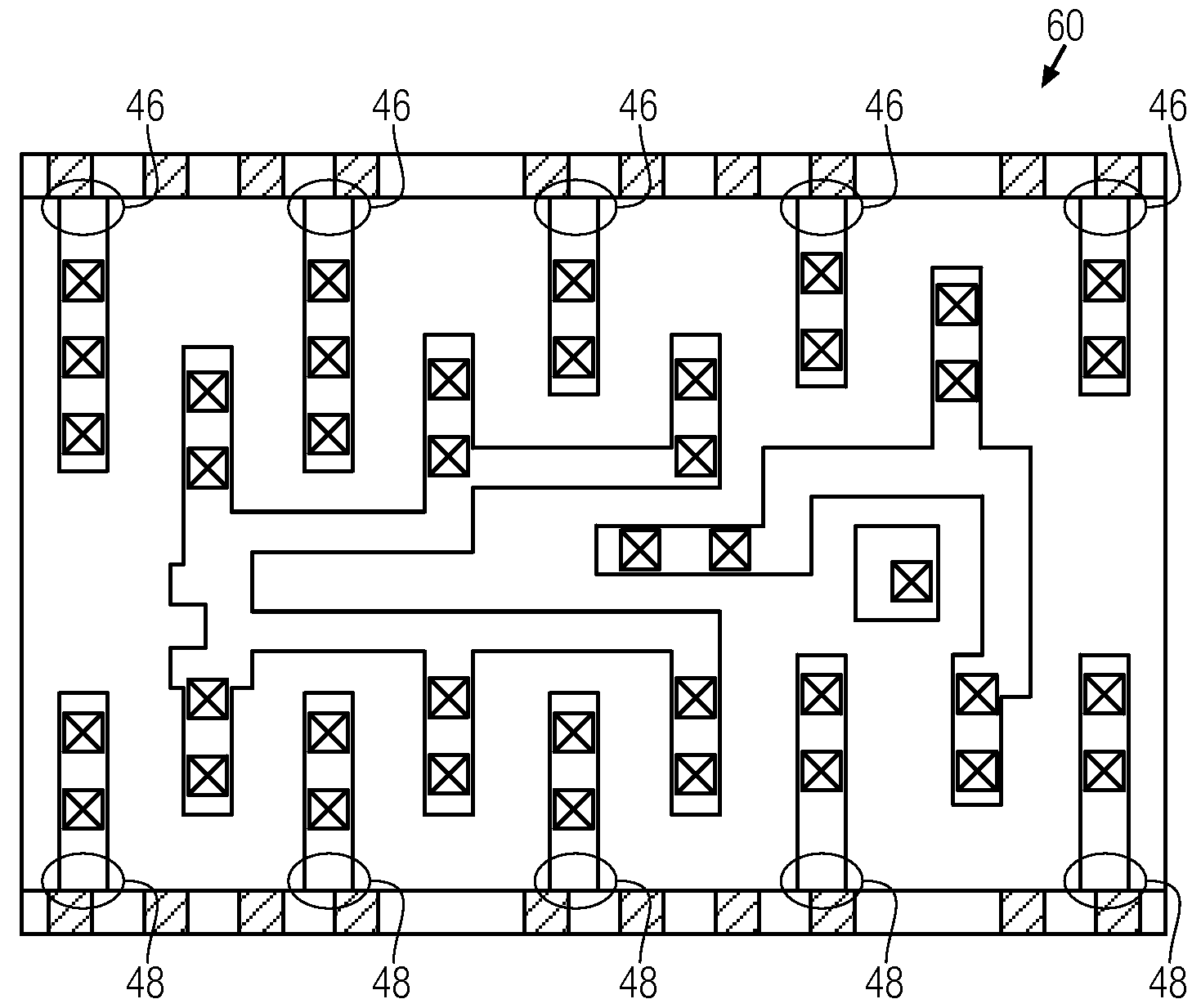
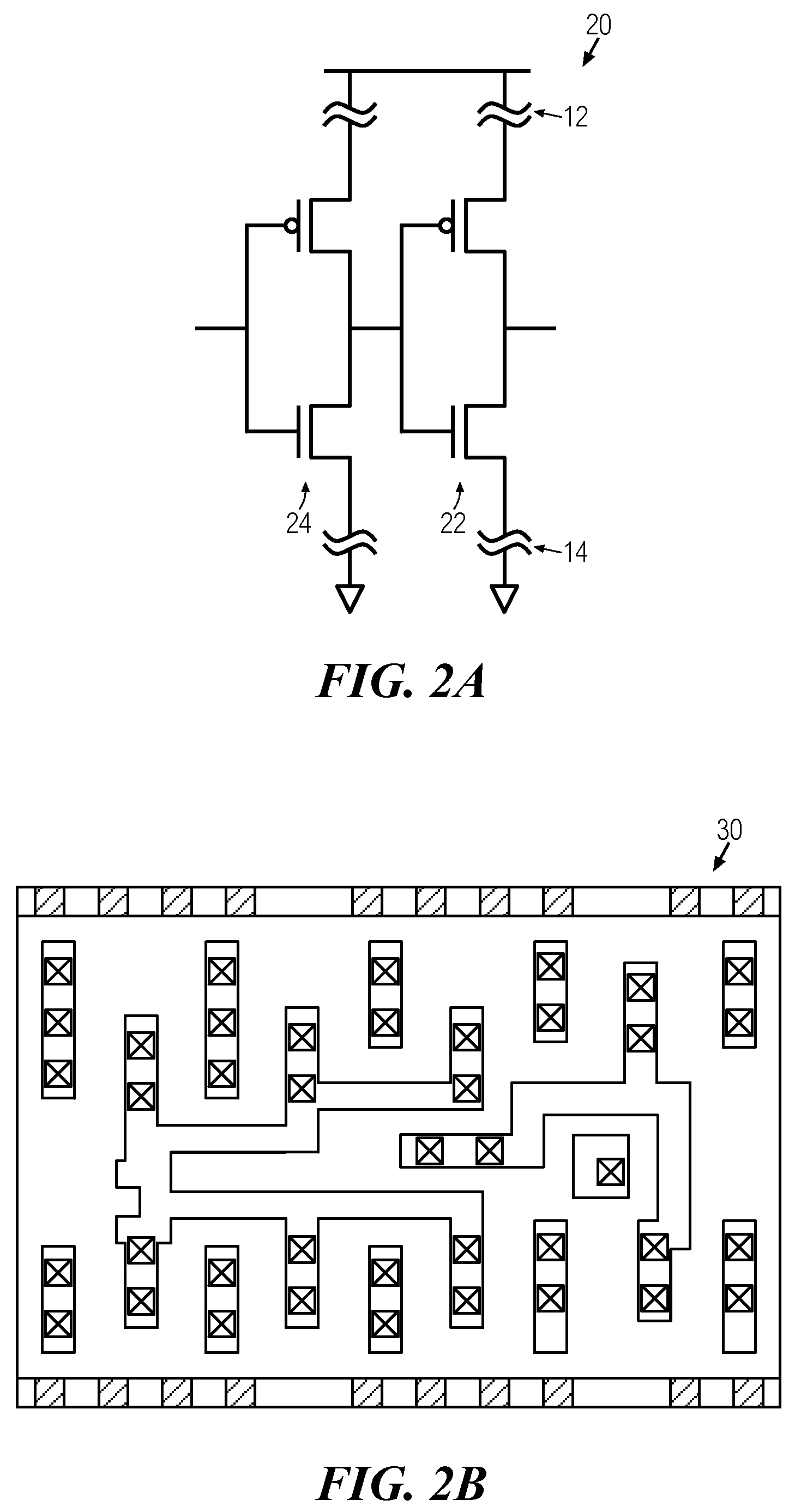
[0017]An aspect of the invention provides a cell based design layout of an integrated circuit having a function, the layout comprising a plurality of cell based base logic cells each having interconnected transistors to perform a logic function; a plurality of additional cells each having at least one transistor and having the power source unconnected to the additional cell, and the plurality of additional cells functionally unconnected to the plurality of base logic cells.

[0018]In an embodiment the at least one additional cell of the plurality of additional cells may have the power source interconnected to the additional cell, and the at least one additional cell may be functionally interconnected to the base logic cells. The additional cell may have at least one transistor having the source unconnected to the power supplies Vss and Vdd, and is functionally unconnected to the plurality of base logic cells. An additional cell may have the source of the at least one transistor interc...


PUM


Abstract

A cell based design layout of an application specific integrated circuit (ASIC) having a function has reduceddecreased power leakage because functionally unconnected additional cells or spare cells of the integrated design layout are unconnected to the power supplies Vdd and Vss.

Description

BACKGROUND OF THE INVENTION[0001]The present invention relates generally to a cell based application specific integrated circuit (ASIC) layout design and more particularly to reducing power consumption in an ASIC having a layout design with a spare cell or spare cell library layout design.[0002]Traditional cell based ASIC layout designs typically include a base set of functional logic cells that are interconnected to perform the desired function of the ASIC. In particular, ASIC layout designs are common in very large scale integration (VLSI) of complex integrated circuits such as processors. In addition to the base set of functional logic cells, the ASIC layout designs typically comprise a plurality of spare cells that are randomly dispersed throughout the functional logic base set of cells. The spare cells may collectively form a spare cell library. The spare cells may be standard library cells. After a metallization process, the spare cells are not connected to the base set of fun...

Claims


Application Information

Patent Timeline
IPC IPC(8): H03K19/177H01L21/82
CPCH03K19/1735H03K19/173
Inventor JAIN, SIDDHARTHAAGARWAL, GAURAVDESAI, ANKITSHARMA
Owner FREESCALE SEMICON INC
Learn More