Device and method for controlling frame input and output
- Summary
- Abstract
- Description
- Claims
- Application Information
AI Technical Summary
Benefits of technology
Problems solved by technology
Method used
Image
Examples
first embodiment
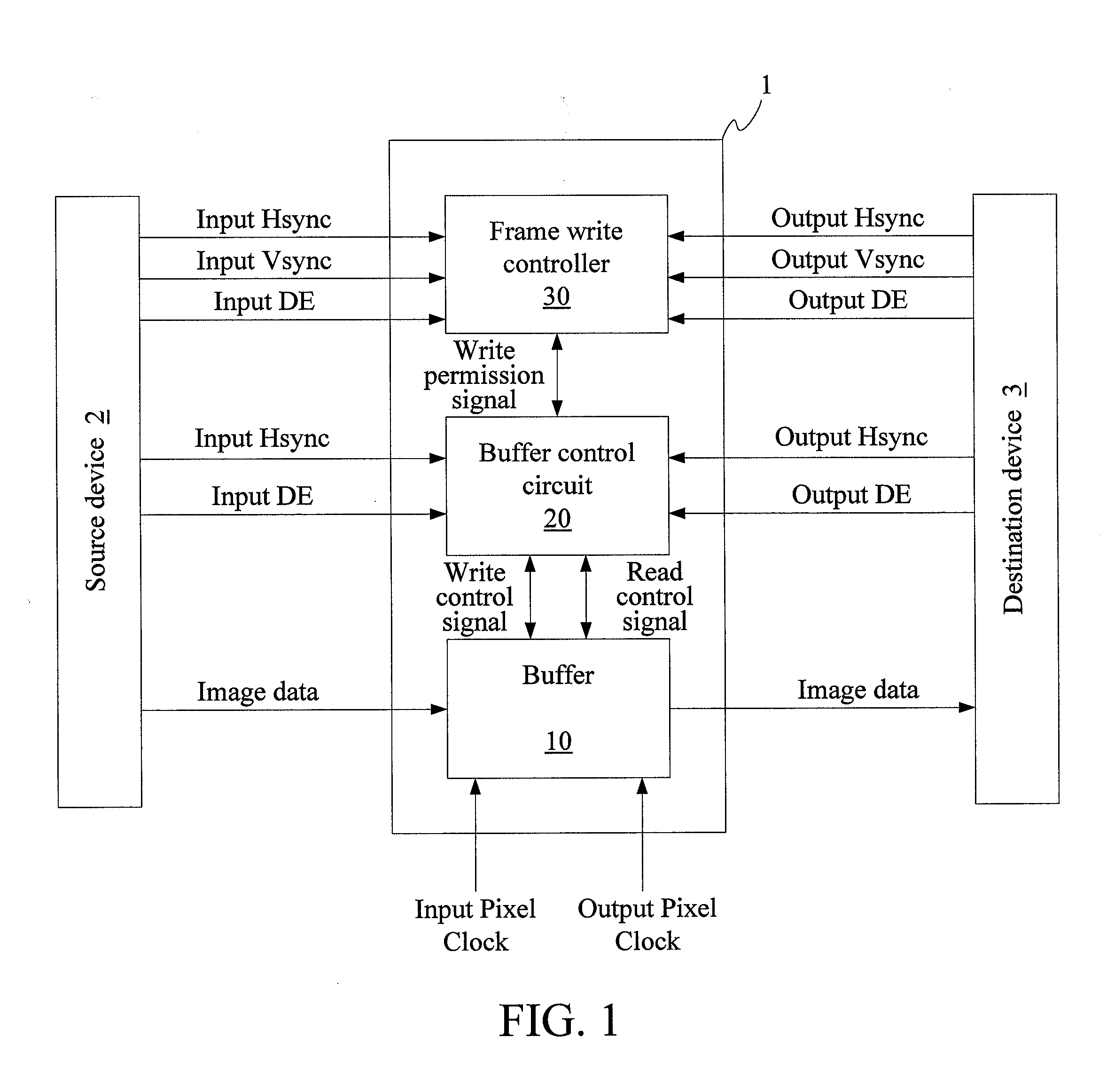
[0021]FIG. 1 is a block diagram of a device for controlling frame input and output according to a The device for controlling frame input and output 1 of the embodiment includes a buffer 10, a buffer control circuit 20, and a frame write controller 30.
[0022]As shown in FIG. 1, the device for controlling frame input and output 1 receives image data from the source device 2 and outputs the image data to a destination device 3 for displaying. The image data includes a plurality of frames, which may also be fields. The source device 2 provides input control parameters (for example, at least one of an input vertical synchronization parameter (Input Vsync), an input horizontal synchronization parameter (Input Hsync), and an input data enabling parameter (Input DE)) and an input pixel clock to the device for controlling frame input and output 1. The source device 2 may provide the input control parameters directly to the device for controlling frame input and output 1. Alternatively, the s...
second embodiment
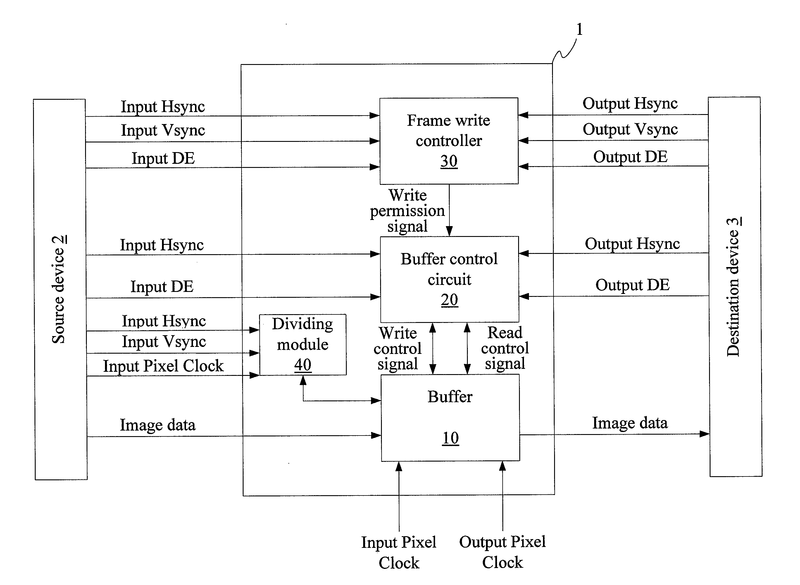
[0090]FIG. 5 is a block diagram of a device for controlling frame input and output according to a A difference between this embodiment and the embodiment in FIG. 1 is that a dividing module 40 is further included. The dividing module 40 calculates a size of an input frame according to an input control parameter (such as, an Input Hsync, an Input Vsync, or an input pixel clock). Next, it is determined whether it is suitable to divide the buffer 10 into two or more frame buffer areas according to the size of the input frame and a storage capacity of the buffer 10. When the size of the input frame is 1 / n (for example, ½) of the storage capacity of the buffer 10, the dividing module 40 is determined to divide the buffer 10 into n frame buffer areas (for example, two frame buffer areas), and each frame buffer area stores one input frame. In this manner, the space of the buffer 10 is fully utilized in the case that the size of the input frame is relatively small, and two or more frame bu...
PUM
 Abstract
Description
Claims
Application Information
 - R&D
- Intellectual Property
- Life Sciences
- Materials
- Tech Scout
- Unparalleled Data Quality
- Higher Quality Content
- 60% Fewer Hallucinations
Browse by: Latest US Patents, China's latest patents, Technical Efficacy Thesaurus, Application Domain, Technology Topic, Popular Technical Reports.
© 2025 PatSnap. All rights reserved.Legal|Privacy policy|Modern Slavery Act Transparency Statement|Sitemap|About US| Contact US: help@patsnap.com


