Nanowire- based solar cell structure

Inactive Publication Date: 2010-07-29
QUNANO
View PDF13 Cites 52 Cited by
  • Summary
  • Abstract
  • Description
  • Claims
  • Application Information

AI Technical Summary

Benefits of technology

[0016]One advantage of the invention is that the solar cell structure allows heterostructures with no need for lattice matching, allowing a large degree of freedom in the choice of materials combinations. In principle there is no limit to the number of different band gaps, i.e. segments in the nanowire, giving the possibility to absorb the whole useful part of, or a selected portion of, the solar spectrum.
[0017]Due to the small growth area used for each individual wire, there is no need for extremely homogeneous growth over a whole wafer, which relaxes the requirements on the growth system. Also due to the small area, the substrate may be polycrystalline or thin-film silicon, or the like.
[0018]One advantage of the solar cell structure according to the first aspect of the invention is that the light guiding shell directs the light in an orderly fashion through regions of decreasing bandgap, allowing sequential light harvesting.
[0019]Further, the light guide structure provides intrinsic concentration of photons into the nanowire, giving a saturated voltage even under diffuse light conditions.
[0020]A still further advantage afforded by the invention is the possibility to use metallic segments to connect the segments of the nanowire. This is not possible in the prior art planar devices as metallic layers are not transparent. However, in the present invention, with the narrow light absorbing nanowire enclosed by a light guiding shell, non-transparency will have limited negative effect.
[0021]By placing the nanowires sufficiently close together on the substrate according to the second aspect of the invention the advantages of using nanowires is combined with an effective absorption of the light, as the incoming light “sees” the closely packed nanowires as a continuous effective medium.

Problems solved by technology

The theoretical limit for the power conversion efficiency of a solar cell based on a single semiconductor material is 31%.
However, fabrication of all the necessary different material combinations is challenging and a high material quality of the crystals is essential for achieving high efficiencies.
The availability of Ge in the Earth's crust is limited and it is expensive, and if such high efficiency tandem solar cells were used in large quantities on earth, this could be a limitation.
However, technical barriers for planar III-V multi junction solar cells can be identified.
Efficiencies above 50% will be very difficult to reach due to physical limitations.
This makes up-scaling to large area substrates extremely challenging, even if such substrates were available at reasonable cost.
Even if these problems could be overcome, the limited number of materials that both have the right band gaps and are more or less lattice matched makes it very difficult to produce more than three junctions in planar solar cells, which is necessary for reaching very high efficiencies.
In addition to the above technical challenges, which are associated with the prior art multi junction cell, both cost and scaling present problems.
By way of example multi-junction cells grown on Ge or III-V substrates are very expensive due to the high substrate costs and the small wafer sizes.
Moreover, III-V materials are today epitaxially grown in high-grade MOCVD or even MBE reactors with low throughputs and the high cost of the precious raw materials makes the use of optical concentrators necessary to improve the cost-performance ratio on the system level.

Method used


Image

  • Nanowire- based solar cell structure
  • Nanowire- based solar cell structure
  • Nanowire- based solar cell structure

Examples


Embodiment Construction

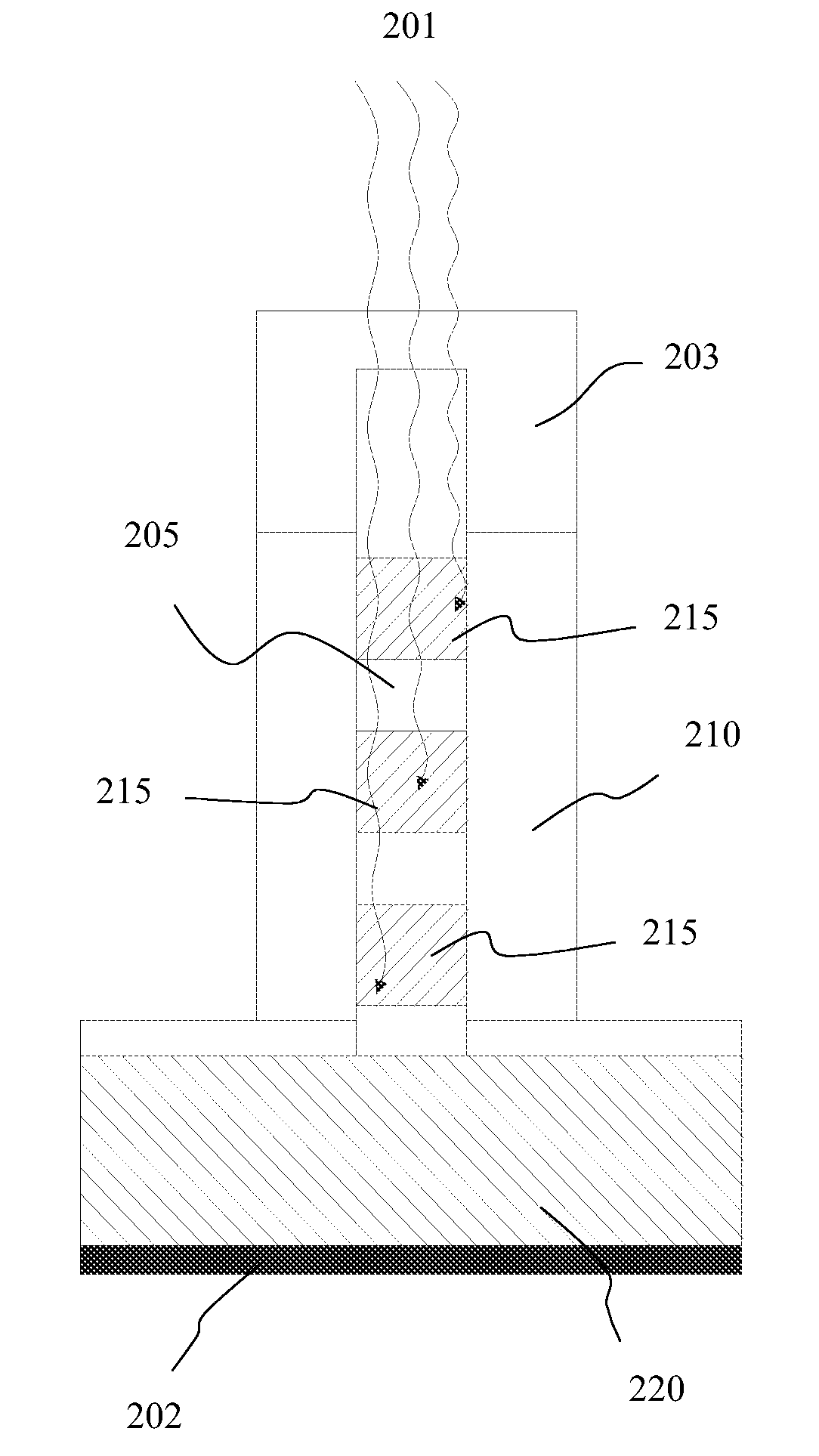
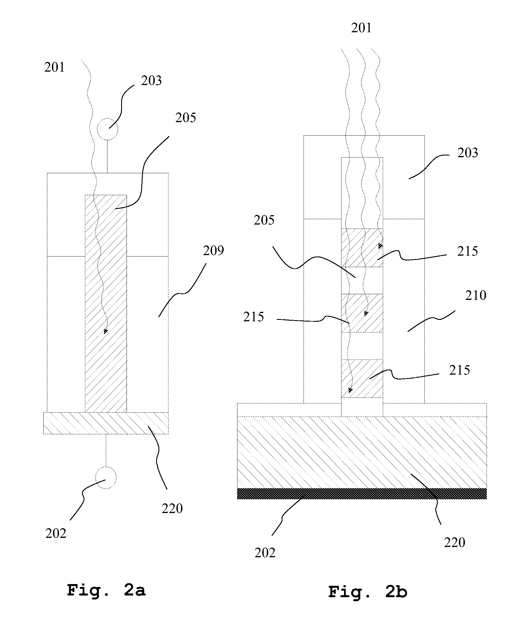
[0035]FIG. 2a schematically illustrates one embodiment of a solar cell structure according to the present invention. A nanowire 205 constitutes the light absorbing part of the solar cell structure and a passivating shell 209 encloses at least a portion of the nanowire 205. Preferably the nanowire protrudes from a substrate 220. The nanowires may protrude substantially perpendicular to the substrate 220 or at an angle.

[0036]Incoming (sun)light 201 is coupled into the nanowire 205 of the solar cell structure. The incoming light generates electron-hole-pairs and preferably the light absorbing part of the solar cell structure, i.e. the nanowire 205, is configured as a pn-junction to establish an electrical field that promotes a current to flow in only one direction through the nanowire 205 between a front contact 203 and a back contact 202. By way of example the front contact 203 and the back contact 202 are respectively, as schematically illustrated in FIG. 2a, electrically connected t...


PUM


Abstract

The solar cell structure according to the present invention comprises a nanowire (205) that constitutes the light absorbing part of the solar cell structure and a passivating shell (209) that encloses at least a portion of the nanowire (205). In a first aspect of the invention, the passivating shell (209) of comprises a light guiding shell (210), which preferably has a high- and indirect bandgap to provide light guiding properties. In a second aspect of the invention, the solar cell structure comprises a plurality of nanowires which are positioned with a maximum spacing between adjacent nanowires which is shorter than the wavelength of the light which the solar cell structure is intended to absorbin order to provide an effective medium for light absorption. Thanks to the invention it is possible to provide high efficiency solar cell structures.

Description

TECHNICAL FIELD OF THE INVENTION[0001]The present invention relates to a solar cell structure. In particular the invention relates to a solar cell structure comprising a nanowire as an active component.BACKGROUND OF THE INVENTION[0002]Interest in solar cell technology has been increasing over the last years. Increasing energy costs as well as environmental concerns are factors behind this interest. Also technology breakthroughs, indicating the possibilities for large scale production of high efficiency solar cells have been important factors.[0003]The most highly efficient existing solar cells are made of III-V semiconductors, such as GaInP or GaInAs, in multi junction cells with several layers each absorbing different parts of the solar spectrum. The advantage of this concept is illustrated by FIG. 1 showing the part of the solar AM1.5 spectrum that can be converted into electrical energy by a typical silicon photo voltaic (PV) cell compared to a GaInP / GaInAs / Ge tandem structure.[0...

Claims


Application Information

Patent Timeline
IPC IPC(8): H01L31/00
CPCH01L31/0304Y02E10/52H01L31/035281H01L31/03529H01L31/0725H01L31/0735H01L31/184H01L31/1844H01L31/1852Y02E10/544H01L29/885H01L31/0547G02B6/0096H01L31/035227H01L31/03046
Inventor SAMUELSON, LARSMAGNUSSON, MARTINCAPASSO, FEDERICO
Owner QUNANO
Why Eureka
Try Eureka